Manufacture method of trench transistor

A technology of trench transistors and manufacturing methods, which is applied in semiconductor/solid-state device manufacturing, electrical components, circuits, etc., can solve the problems of unfavorable mass production, device size cannot be reduced according to demand, and expensive manufacturing cost, etc., and achieve low saturation voltage The effect of reducing, reducing the number of mask plates, and avoiding the limitation of alignment deviation

Active Publication Date: 2015-04-08
SHANGHAI HUAHONG GRACE SEMICON MFG CORP
View PDF4 Cites 0 Cited by
  • Summary
  • Abstract
  • Description
  • Claims
  • Application Information

AI Technical Summary

Problems solved by technology

The alignment deviation between different masks will make the device size unable to be reduced according to the demand, and the more precise photolithography technology makes the manufacturing cost expensive, which is not conducive to mass production

Method used


Image

  • Manufacture method of trench transistor
  • Manufacture method of trench transistor
  • Manufacture method of trench transistor

Examples


Embodiment Construction

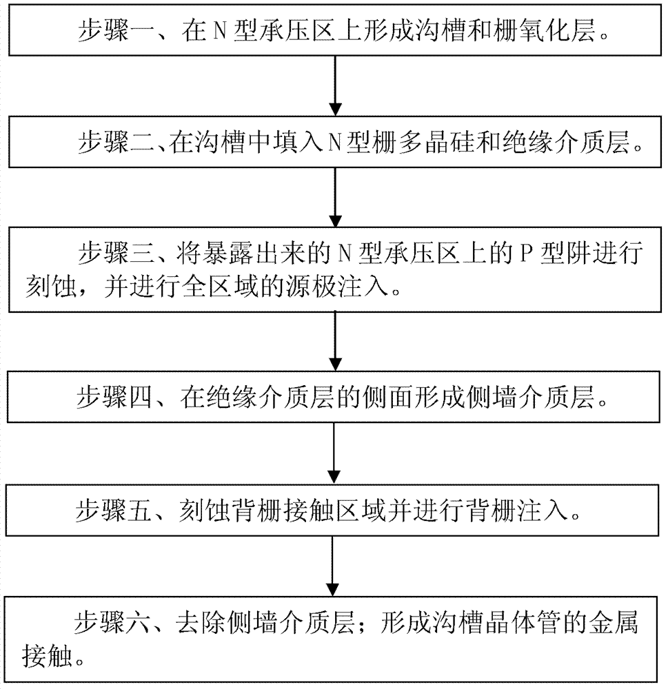
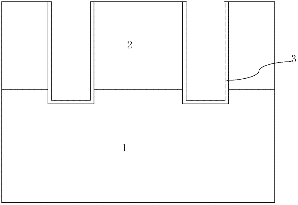
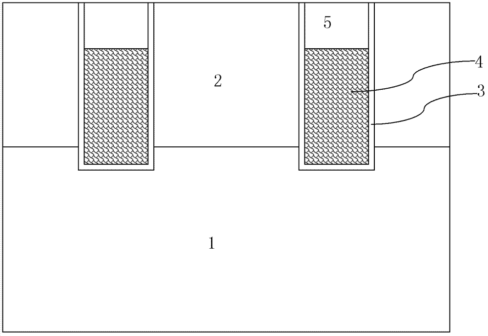
[0022] Such as figure 1 Shown is the flow chart of the method of the embodiment of the present invention; Figure 2 to Figure 7 Shown is a schematic diagram of the device structure in each step of the method of the embodiment of the present invention. The manufacturing method of the trench transistor according to the embodiment of the present invention includes the following steps:

[0023] Step 1, such as figure 2 As shown, a trench is formed on the N-type pressure-bearing region 1 with a P-type well 2 formed on the top, the groove passes through the P-type well 2 and enters into the N-type pressure-bearing region 1, in the The bottom and sidewall surfaces of the trench form gate oxide layer 3 .

[0024] When the trench transistor is a silicon-based device, the N-type pressure receiving region 1 is made of silicon material, such as silicon epitaxial layer, or Czochralski single crystal silicon, or zone-fused single crystal silicon. Alternatively, when the trench transist...


PUM


Abstract

The invention discloses a manufacture method of a trench transistor. The manufacture method includes: subjecting a source electrode region to etching and source electrode implantation by forming insulating medium layers on the top of gate polycrystalline silicon and using the insulating medium layers as masks, and subjecting a back gate contact region to etching and back gate implantation by forming spacer medium layers on the side faces of the insulating medium layers and using the insulating medium layers and the spacer medium layers as masks. Therefore, the number of masks required by the front-side process can be decreased, production cost can be lowered, and limitations of different masks on alignment errors can be avoided, and further, the size of the trench transistors is further deceased, the density of trench transistors in a chip is increased, and the trench transistors lower in breakover resistance and saturation voltage drop and higher in current driving capacity are obtained beneficially.

Description

technical field [0001] The invention relates to a semiconductor integrated circuit manufacturing process method, in particular to a trench transistor manufacturing method. Background technique [0002] In the application of power and high-voltage devices, it is hoped that the on-resistance of the transistor will be smaller, the saturation voltage drop will be lower, and the current driving capability will be greater. How to integrate more devices within a certain chip area is particularly important. The gates of the existing vertical double diffused field effect transistor (VDMOS) and the existing insulated gate bipolar transistor (IGBT) are all formed in the trench and have a similar front structure. Various corresponding masks are used in the source, back gate and other processes of trench transistors. Alignment deviation between different masks will prevent device size from being reduced according to demand, and more precise photolithography technology makes manufacturin...

Claims


Application Information

Patent Timeline
Patent Type & Authority Patents(China)
IPC IPC(8): H01L21/336H01L21/331
Inventor 韩峰段文婷
Owner SHANGHAI HUAHONG GRACE SEMICON MFG CORP
Why Eureka
Try Eureka