

Electrostatic chuck and semiconductor/liquid crystal manufacturing equipment
An electrostatic chuck and manufacturing device technology, which is applied in semiconductor/solid-state device manufacturing, electrostatic attraction holding device, positioning device, etc., can solve the problems of lower pass rate, worse production efficiency, lower throughput, etc., and achieve Ensure the uniformity of temperature, improve production efficiency, and improve the effect of pass rate
- Summary
- Abstract
- Description
- Claims
- Application Information
AI Technical Summary
Problems solved by technology
Method used
Image

Examples
no. 1 Embodiment approach
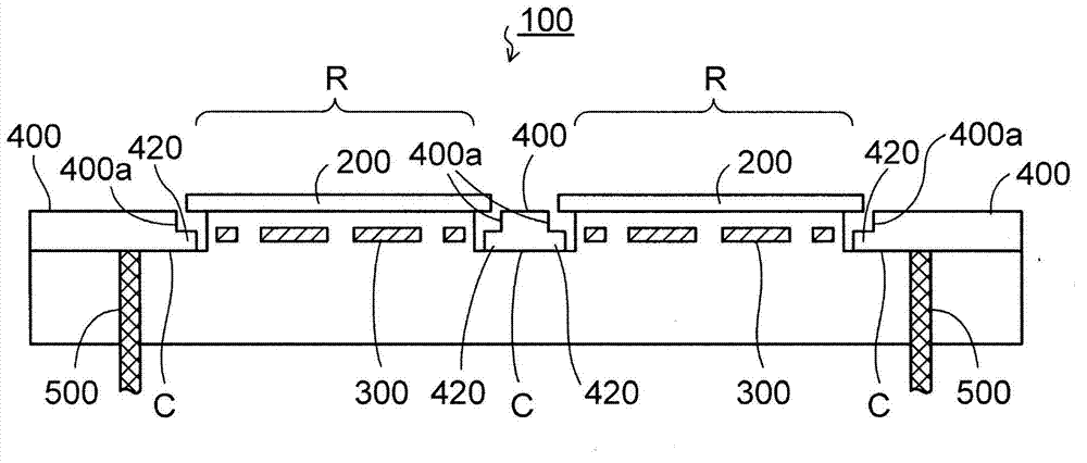
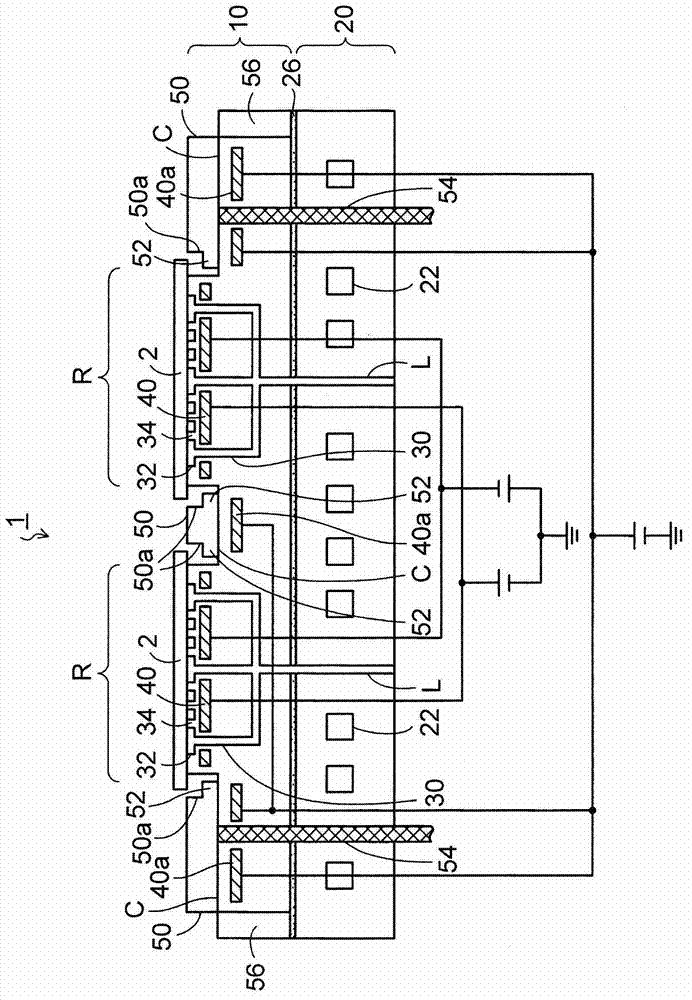
[0042] image 3 is a sectional view showing the electrostatic chuck according to the first embodiment, Figure 4 It is a plan view showing the electrostatic chuck of the first embodiment.
[0043] Such as image 3 As shown, the electrostatic chuck 1 of the first embodiment includes a substrate 20 and a chuck function part 10 bonded to the substrate 20 with an adhesive 26 such as silicone resin.
[0044] The substrate 20 is formed of metal such as aluminum, for example, and a cooling water channel 22 is provided inside as a cooling mechanism. The chuck function part 10 is formed of ceramics such as alumina, for example, and has a plurality of chuck regions R on which wafers (attracted objects) are placed on the surface.
[0045] In each chuck region R, a gas hole 30 for supplying heat transfer gas and a concave portion 32 communicating with the gas hole 30 and extending in the horizontal direction are provided on the surface, and a plurality of convex portions are arranged i...
no. 2 Embodiment approach
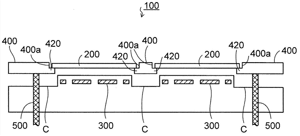
[0071] Figure 6 It is a sectional view showing the electrostatic chuck according to the second embodiment.
[0072] of the above-mentioned first embodiment image 3 The electrostatic chuck 1 has a structure in which heat transfer gas is not supplied between the tray 50 and the electrostatic chuck 1 . The second embodiment is characterized in that cooling efficiency can be improved even if heat transfer gas is supplied between the tray and the electrostatic chuck. exist Figure 6 In the description, the same reference numerals are assigned to the same elements as those in the first embodiment, and detailed description thereof will be omitted.
[0073] Such as Figure 6 As shown, in the electrostatic chuck 1a of the second embodiment, the air hole 30a for supplying the heat transfer gas and the recessed portion 32a communicating with the air hole 30a are also provided on the surface where the concave portion C of the tray 50 is disposed. The air hole 30 a of the concave po...
no. 3 Embodiment approach
[0077] Figure 7 It is a sectional view showing the electrostatic chuck according to the third embodiment. exist Figure 7 In the description, the same reference numerals are assigned to the same elements as those in the first embodiment, and detailed description thereof will be omitted.
[0078] Such as Figure 7 Like the electrostatic chuck 1b shown, the gas path L1 including the gas hole 30 for supplying the heat transfer gas to the wafer 2 and the gas path L2 including the gas hole 30a for supplying the heat transfer gas to the tray 50 can be separated into independent from each other. line.
[0079] In this way, since the flow rate and gas pressure of the heat transfer gas can be adjusted independently between the wafer 2 and the tray 50 , the cooling efficiency can be changed between the wafer 2 and the tray 50 . For example, when it is necessary to cool the tray 50 more aggressively than the wafer 2 in order to realize the etching characteristic or the stability of ...
PUM
 Abstract
Description
Claims
Application Information