Flexible display substrate and preparation method thereof as well as flexible display device
A flexible display and substrate technology, applied in nonlinear optics, climate sustainability, final product manufacturing, etc., can solve the problems of flexible display substrate damage, reduced display performance, small deformation, etc., to avoid failure or wear, preparation Simple process and large deformation effect
- Summary
- Abstract
- Description
- Claims
- Application Information
AI Technical Summary
Problems solved by technology
Method used
Image
Examples
Embodiment 1
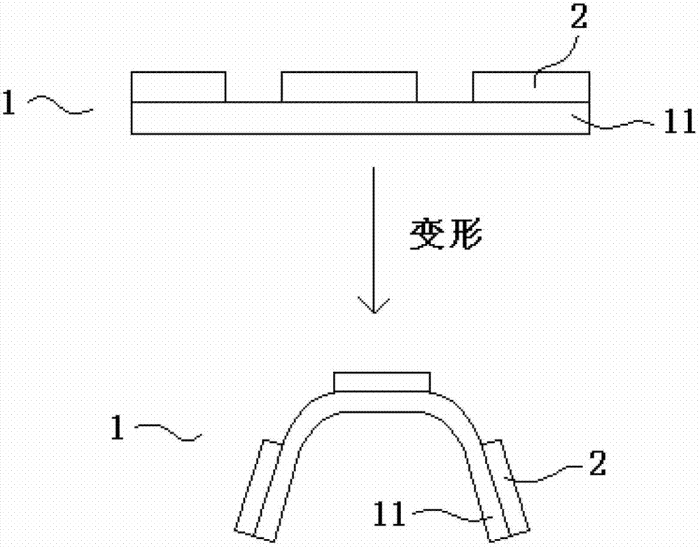
[0046] Such as figure 1 As shown, this embodiment provides a flexible display substrate 1 , which includes a hard material layer 2 disposed at a vulnerable position of the flexible display substrate 1 .
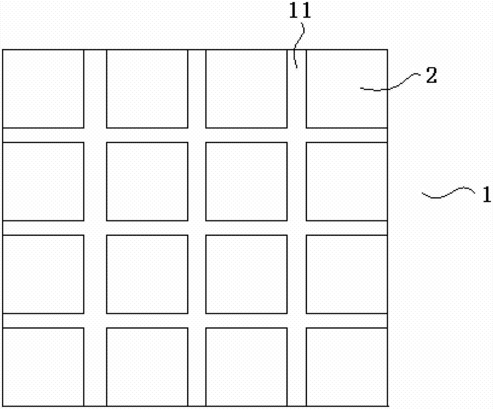
[0047] In this embodiment, the flexible display substrate 1 is provided with a hard material layer 2 at the vulnerable position, that is, the hard material layer 2 forms a structure similar to a "scale", so the flexible display substrate 1 has an alternating soft and hard structure as a whole. When the display substrate 1 is bent, the deformation is mainly concentrated in the part without the hard material layer 2 (or concentrated in the gap between the "scales"), so as long as the hard material layer 2 is placed on the vulnerable structure, due to The protective effect of the hard material layer 2 on the vulnerable structure is to prevent the vulnerable structure from being deformed or deformed very little, thereby avoiding its failure or wear, and at the same time avoiding ...
Embodiment 2
[0049] Such as Figure 2 to Figure 9 As shown, this embodiment provides a flexible display substrate 1 , which includes a base 11 and a display structure 12 disposed on the base 11 , and has a hard material layer 2 at a vulnerable position of the flexible display substrate 1 .
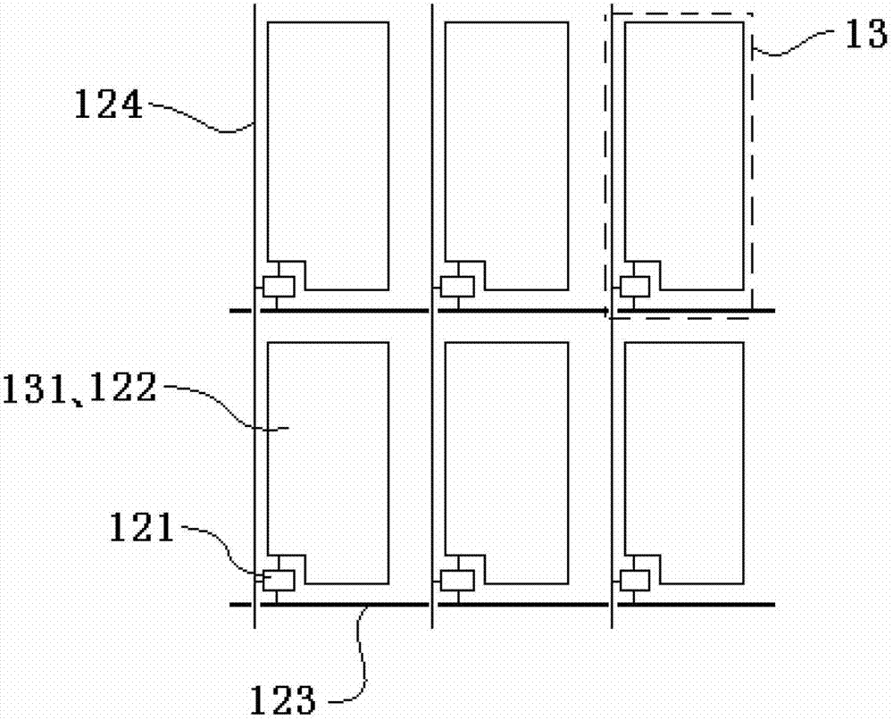
[0050] Wherein, the display structure 12 includes thin film transistors 121, leads, pixel electrodes 122, cathodes, anodes, electroluminescent layers, electrophoretic capsules, black matrixes, color filters, polarizers and other structures for displaying on the substrate 11. It can be divided into multiple layers (for example, the thin film transistor 121 includes a gate layer, an insulating layer, a source / drain layer, an active layer, a passivation layer, etc.).
[0051] Since the flexible display substrate 1 of this embodiment has a hard material layer 2 at the vulnerable position, when the flexible display substrate 1 is bent, the deformation mainly concentrates on the area without the hard materia...
Embodiment 3
[0076] This embodiment provides a method for preparing a flexible display substrate, which includes:
[0077] Patterns of the hard material layer are formed at vulnerable positions of the base of the flexible display substrate.
[0078] The preparation method of the flexible display substrate of this embodiment includes the step of forming a hard material layer on the vulnerable position of the substrate, that is, it prepares the above-mentioned flexible display substrate, so it is not easy to damage, has a large amount of deformation, good display performance, and low cost. Low, simple preparation process.
[0079] Preferably, the hard material layer can be formed by patterning process, inkjet printing process, screen printing and so on.
[0080] Among them, the "patterning process" usually includes steps such as photoresist coating, exposure, development, etching, and photoresist stripping, which are known processes for forming specific patterns; When patterning, the etchi...
PUM
 Abstract
Description
Claims
Application Information


