Aluminum grid and preparation method thereof as well as thin film transistor with aluminum grid
A technology of aluminum thin film and aluminum gate, which is applied to transistors, semiconductor devices, electrical components, etc., can solve the problems of easy corrosion and easy generation of hillocks on aluminum gates, and achieves the effects of easy implementation, small delay time, and low resistance.
- Summary
- Abstract
- Description
- Claims
- Application Information
AI Technical Summary
Problems solved by technology
Method used
Image


Examples
Embodiment 1
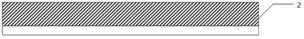
[0050] Such as figure 1 As shown, this embodiment provides an aluminum gate, including an aluminum gate body formed on a substrate; a first cover layer 1 disposed on the upper surface of the aluminum gate body opposite to the substrate; It also includes a second cover layer 7 wrapped around the aluminum gate body, and the second cover layer 7 is seamlessly connected with the first cover layer 1; the first cover layer 1 and the The second cover layer 7 is made of metal with thermal expansion coefficient less than 20. The aluminum gate body in this embodiment is completely covered by the first capping layer 1 and the second capping layer 7. Since the thermal expansion coefficient of the metal is small, it is not easy to be thermally expanded. Therefore, under high-temperature processes, such as LTPS (low temperature polysilicon ) in the activation process, the process temperature is as high as 450°C, the compressive stress in the aluminum film is absorbed by the metal cap laye...
Embodiment 2
[0062] On the basis of embodiment 1, the present embodiment also includes the following steps:
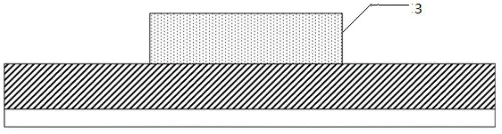
[0063] S4, forming a gate pattern on the metal layer, etching away the metal layer outside the gate pattern, to obtain the first capping layer 1 covering the upper surface of the aluminum gate body and covering the aluminum gate body. The second cover layer 7 around the gate body; the etching method is dry etching or wet etching.
[0064] Similar to Embodiment 1, in this embodiment, a gate pattern is formed on the metal layer by photolithography. Moreover, during photolithography, the critical dimension of the photomask is controlled to be smaller than the critical dimension of the aluminum gate. In this embodiment, keep the exposure energy 100-110mj / cm2 and the photoresist thickness 1400-1600nm unchanged, and the exposure time is 350-450ms. Preferably, keep the exposure energy 100mj / cm2 and the photoresist thickness 1400nm unchanged, and the exposure time is 350ms.
PUM
| Property | Measurement | Unit |
|---|---|---|
| Thickness | aaaaa | aaaaa |
| Thickness | aaaaa | aaaaa |
Abstract
Description
Claims
Application Information
 - R&D
- Intellectual Property
- Life Sciences
- Materials
- Tech Scout
- Unparalleled Data Quality
- Higher Quality Content
- 60% Fewer Hallucinations
Browse by: Latest US Patents, China's latest patents, Technical Efficacy Thesaurus, Application Domain, Technology Topic, Popular Technical Reports.
© 2025 PatSnap. All rights reserved.Legal|Privacy policy|Modern Slavery Act Transparency Statement|Sitemap|About US| Contact US: help@patsnap.com