Method and equipment for purifying polycrystalline silicon through solidification crucible rotary electron beam melting

An electron beam smelting, polysilicon technology, applied in chemical instruments and methods, silicon compounds, inorganic chemistry, etc., can solve the problems of inability to realize continuous feeding and continuous discharging, increase the time for multiple smelting, and be unfavorable for industrialized production. Reduced purification time, compact structure, increased continuity and stability

Inactive Publication Date: 2013-03-27
QINGDAO NEW ENERGY SOLUTIONS
View PDF5 Cites 17 Cited by
  • Summary
  • Abstract
  • Description
  • Claims
  • Application Information

AI Technical Summary

Problems solved by technology

Electron beam smelting technology is one of the important methods in the metallurgical preparation of solar-grade polysilicon. It is a process that uses high-energy-density electron beams as a melting heat source. The general electron beam smelting method is to form a molten pool by melting bulk silicon materials. Finally, under the high temperature generated by the electron beam, the surface evaporation effect is used to effectively remove impurities with high saturated vapor pressure such as phosphorus and aluminum. , take out the solidified ingot, and then carry out the next smelting, so that the vacuum of the extraction chamber and the electron gun preheating must be repeated, which not only increases the time of multiple smelting, but also increases energy consumption, such as power and equipment loss etc., resulting in a reduction in production efficiency. At the same time, in the previous electron beam melting polysilicon process, continuous feeding and continuous discharging could not be realized, which increased production costs and was not conducive to industrial production.

Method used


Image

  • Method and equipment for purifying polycrystalline silicon through solidification crucible rotary electron beam melting
  • Method and equipment for purifying polycrystalline silicon through solidification crucible rotary electron beam melting

Examples


Embodiment 1

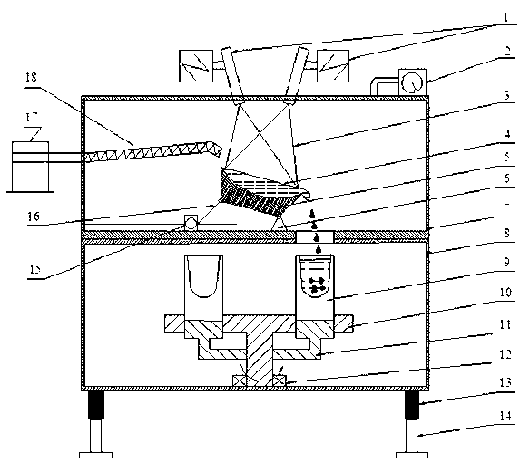
[0023] Such as figure 1 and figure 2 The equipment used in the method of solidifying crucible rotary electron beam melting and purifying polysilicon shown in the figure is composed of an upper chamber 7 and a lower chamber 8 as a whole, the upper chamber 7 is fixedly installed on the ground base support, and the upper chamber Two electron guns 1 are installed on the top of the chamber. The vacuum pump group 2 communicates with the upper chamber 7 through a vacuum pipeline. The vacuum pump group 2 includes a mechanical pump, a Roots pump and a diffusion pump. A vacuum gauge is installed on the vacuum pipeline.

[0024] On the bottom plate of the upper chamber 7, the melting crucible 5 is movably installed through the crucible frame 6, the sliding mechanism 15 is installed on one side of the melting crucible through the transmission rod 16, the charging box 17 is fixedly installed on the side wall of the upper chamber 7, and the feeding belt 18 is fixed Installed on the chargi...

Embodiment 2

[0027] Utilize the electron beam smelting equipment described in embodiment 1 to smelt and purify polycrystalline silicon, concrete steps are as follows:

[0028]The first step of material preparation and pre-treatment: First, use the feeding belt to transport the high-phosphorus silicon material in the charging box with a phosphorus content of 10ppmw to the melting crucible, until the silicon material fills 95% of the volume of the melting crucible, turn on the vacuum pump group, and the chamber The vacuum degree is pumped to 5×10 -2 Pa; preheat the electron gun, set the high voltage to 30kV, and after the high voltage is stable for 10 minutes, turn off the high voltage, set the beam current of the electron gun to 200mA, and perform preheating. After preheating for 10 minutes, turn off the beam current of the electron gun;

[0029] The second step of smelting and purification: turn on the high voltage and beam current of the electron gun at the same time, and after the voltag...

Embodiment 3

[0032] Utilize the electron beam smelting equipment described in embodiment 1 to smelt and purify polycrystalline silicon, concrete steps are as follows:

[0033] The first step of material preparation and pre-treatment: first, use the feeding belt to transport the high-phosphorus silicon material with a phosphorus content of 34ppmw in the charging box to the melting crucible until the silicon material fills 92% of the volume of the melting crucible, turn on the vacuum pump group, and turn on the chamber Medium vacuum pumped to 3×10 -2 Pa; preheat the electron gun, set the high voltage to 31kV, and after the high voltage is stable for 8 minutes, turn off the high voltage, set the beam current of the electron gun to 150mA, and perform preheating. After preheating for 12 minutes, turn off the beam current of the electron gun;

[0034] The second step of smelting and purification: turn on the high voltage and beam current of the electron gun at the same time, after the voltage an...


PUM


Abstract

The invention belongs to the technical field of physical metallurgy technological purification, and in particular relates to a method and equipment for purifying polycrystalline silicon through electron beam melting. A high-phosphorus silicon material is molten through electron beams under the vacuum condition to obtain low-phosphorous molten silicon, and the low-phosphorous molten silicon is poured into a solidification crucible to be solidified; the processes of charging, smelting and purifying and pouring are repeated until the solidification crucible is fully loaded; another hollow solidification crucible is rotated below a molten liquid pouring port, and the processes of charging, smelting and purifying and pouring are repeated until the solidification crucible is fully loaded; and the processes of fully charging one solidification crucible and rotating another hollow solidification crucible below the molten silicon pouring port are repeated until all the solidification crucibles are fully loaded, and after the low-phosphorous molten silicon in all the solidification crucibles is solidified, ingots are taken out. By the method, the whole purifying time of a plurality of times of smelting is reduced, and the times for vacuumizing and preheating of electron guns are reduced, so that the production efficiency is increased; and the equipment is compact in structure, is easy to operate, is safe and controllable and has high production efficiency.

Description

technical field [0001] The invention belongs to the technical field of purifying polysilicon by physical metallurgy technology, in particular relates to a method for purifying polysilicon by electron beam smelting, and also relates to its equipment. Background technique [0002] Solar-grade polysilicon material is the most important photovoltaic material. It is used in solar cells and can convert solar energy into electrical energy. In today's shortage of conventional energy sources, solar energy has huge application value. In recent years, the global solar photovoltaic industry has grown rapidly. Solar cells The rapid increase in output has directly driven the sharp expansion of polysilicon demand. However, the high manufacturing cost and complex manufacturing process of solar-grade polysilicon materials are the bottlenecks restricting the development of the photovoltaic industry, which seriously hinders the promotion and use of solar cells in my country. my country's ...

Claims


Application Information

Patent Timeline
Patent Type & Authority Applications(China)
IPC IPC(8): C01B33/037
Inventor 谭毅姜大川李坚之胡志刚安广野
Owner QINGDAO NEW ENERGY SOLUTIONS
Why Eureka
Try Eureka