Infrared focal plane array detector

An infrared focal plane and array detector technology, which is applied in the field of infrared focal plane array detectors, can solve the problems of high packaging cost, difficult manufacturing process, and large volume, and achieve the effects of reducing packaging cost, simplifying packaging structure, and reducing volume

Inactive Publication Date: 2013-03-27
YANTAI RAYTRON TECH
View PDF3 Cites 15 Cited by
  • Summary
  • Abstract
  • Description
  • Claims
  • Application Information

AI Technical Summary

Problems solved by technology

[0004] There are many internal components in this package structure, for example, it is necessary to integrate a thermoelectric cooler 5 with a volume much larger than that of the chip, so the cavity of the housing 2 is relatively large, and the outgassing rate inside the cavity is also high, requiring a larger volume The getter 7 is electrically activated, and at the same time, the opening area of ​​the shell 2 is also large, and a large optical window 6 is also required to match it, and the cost of the optical window 6 is closely related to its area. The larger the optical window 6, the higher the cost , and this kind of large-area optical window has a large deformation under different operating temperatures, and it is difficult to ensure the long-term life of the packaging structure. In short, this packaging structure makes the packaging cost high, bulky, difficult to manufacture and difficult ensure

Method used


Image

  • Infrared focal plane array detector
  • Infrared focal plane array detector
  • Infrared focal plane array detector

Examples


Embodiment Construction

[0030] The principles and features of the present invention are described below in conjunction with the accompanying drawings, and the examples given are only used to explain the present invention, and are not intended to limit the scope of the present invention.

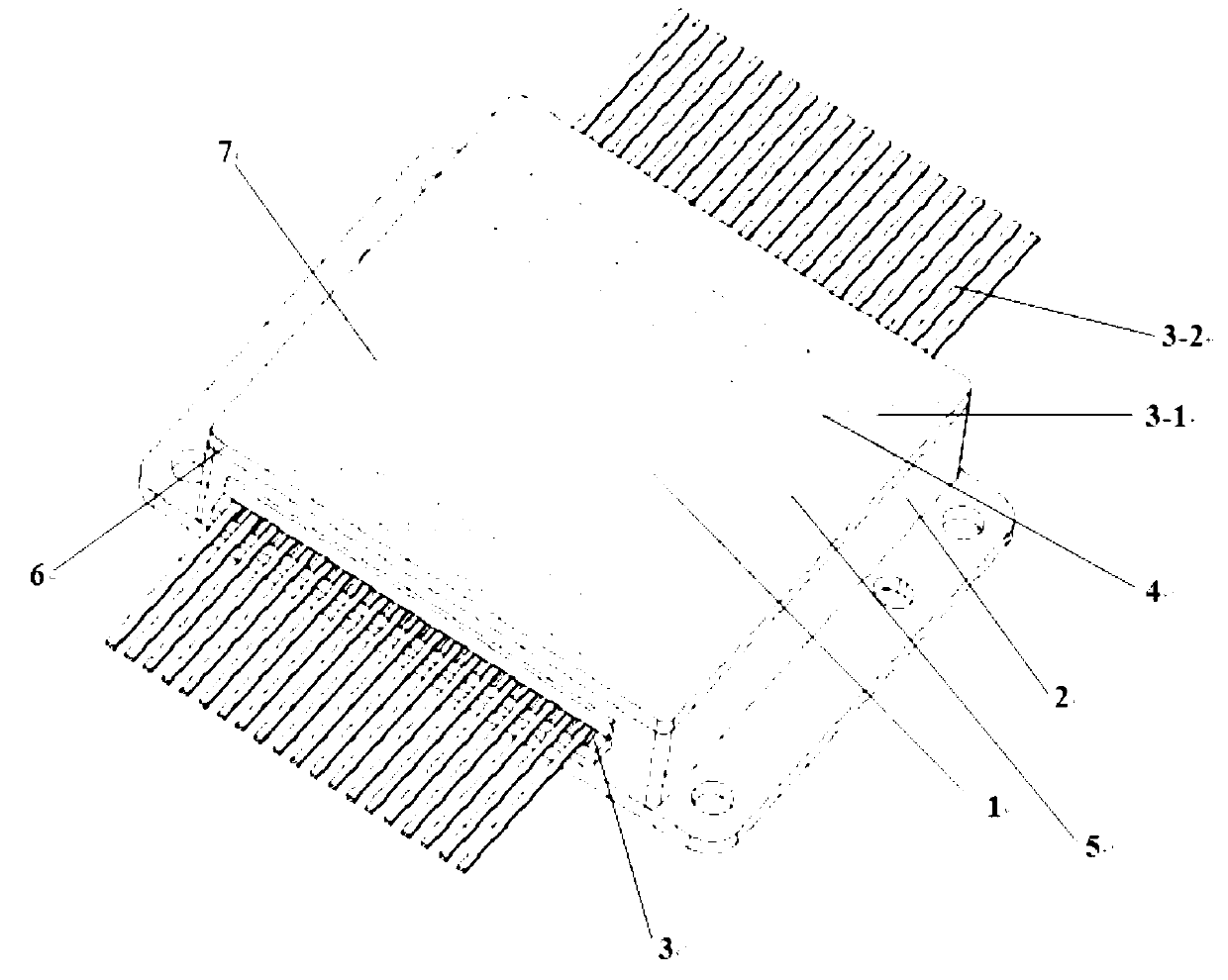
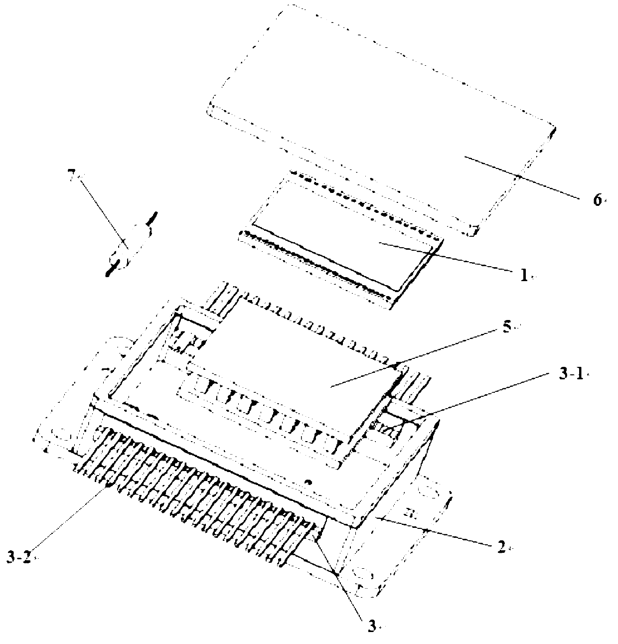
[0031] Generally speaking, the high-vacuum packaging technology of infrared focal plane array detectors uses a metal shell as a sealed cavity, and its typical structure is as follows: figure 1 as shown, figure 2 A schematic diagram of the exploded structure of the typical structure. The shell 2 is a cuboid cavity with an opening, and a ceramic structural part 3 is made on its side wall. The ceramic structural part 3 and the shell 2 are sealed and welded through a metal-ceramic co-firing process. The ceramic structural part 3 is made of The metal pad 3-1, the metal pad 3-1 is electrically connected with the metal lead 3-2 attached to the ceramic structure 3 outside the side wall of the housing 2, so that the infrar...


PUM


Abstract

The invention relates to the field of semiconductor photoelectrons, in particular to an infrared focal plane array detector which comprises an encapsulation casing, an infrared optical window and a buffering ring. The encapsulation casing, the infrared optical window and the buffering ring form a closed vacuum cavity. The buffering ring is positioned between the encapsulation casing and the infrared optical window. An electrical activation getter and an infrared focal plane detector chip are arranged in the vacuum cavity. The encapsulation casing comprises a bottom surface, wherein the infrared focal plane detector chip is arranged on the bottom surface. A welding plate is arranged on the side of the bottom surface, a metal pin is arranged outside the bottom surface, the welding plate is electrically communicated with the metal pin, and the electrical activation getter is electrically communicated with the metal pin. A metal welding plate is arranged on the infrared focal plane detector chip and connected with the welding plate through a metal wire. The encapsulation structure of the infrared focal plane array detector is simplified, the size of the infrared focal plane array detector is reduced, and the encapsulation cost of the infrared focal plane array detector is reduced.

Description

technical field [0001] The invention relates to the field of semiconductor optoelectronics, in particular to an infrared focal plane array detector. Background technique [0002] Infrared imaging technology is more and more widely used in industrial sensing, image monitoring, automobile industry, fire search and rescue, and even military navigation and night vision. Infrared focal plane detector manufacturing technology is the core of thermal imaging technology, and infrared focal plane array detector chip sealing packaging technology is the key link to realize infrared detector imaging, infrared focal plane array detector chip needs to be sealed under high vacuum environment, otherwise the imaging function of its bolometer cannot be exerted. [0003] Generally speaking, the high-vacuum packaging technology of infrared focal plane array detectors uses a metal shell as a sealed cavity, and its typical structure is as follows: figure 1 as shown, figure 2 A schematic diagra...

Claims


Application Information

Patent Timeline
Patent Type & Authority Applications(China)
IPC IPC(8): G01J5/00G01J5/02
Inventor 熊笔锋陈文祥杨秀武
Owner YANTAI RAYTRON TECH
Why Eureka
Try Eureka