Method for regulating structure of nanosphere convex plane array type SERS (Surface Enhanced Raman Scattering) substrate

A planar array, nanosphere technology, applied in microstructure technology, microstructure devices, manufacturing microstructure devices, etc., can solve the problems of small substrate area, difference, difficult high-throughput preparation of high-quality SERS substrates, etc.

Inactive Publication Date: 2013-04-03
JIANGNAN UNIV
View PDF4 Cites 0 Cited by
  • Summary
  • Abstract
  • Description
  • Claims
  • Application Information

AI Technical Summary

Problems solved by technology

However, the types of substrate surface structures reported in the literature are significantly different from each other, the area of ​​substrates is generally small, and some preparation processes require special equipment, which makes it difficult to guide the high-throughput preparation of high-quality SERS substrates

Method used


Image

  • Method for regulating structure of nanosphere convex plane array type SERS (Surface Enhanced Raman Scattering) substrate
  • Method for regulating structure of nanosphere convex plane array type SERS (Surface Enhanced Raman Scattering) substrate
  • Method for regulating structure of nanosphere convex plane array type SERS (Surface Enhanced Raman Scattering) substrate

Examples


Embodiment 1

[0016] Example 1 Preparation and Structural Characterization of Nanosphere Convex Plane Array SERS Substrate

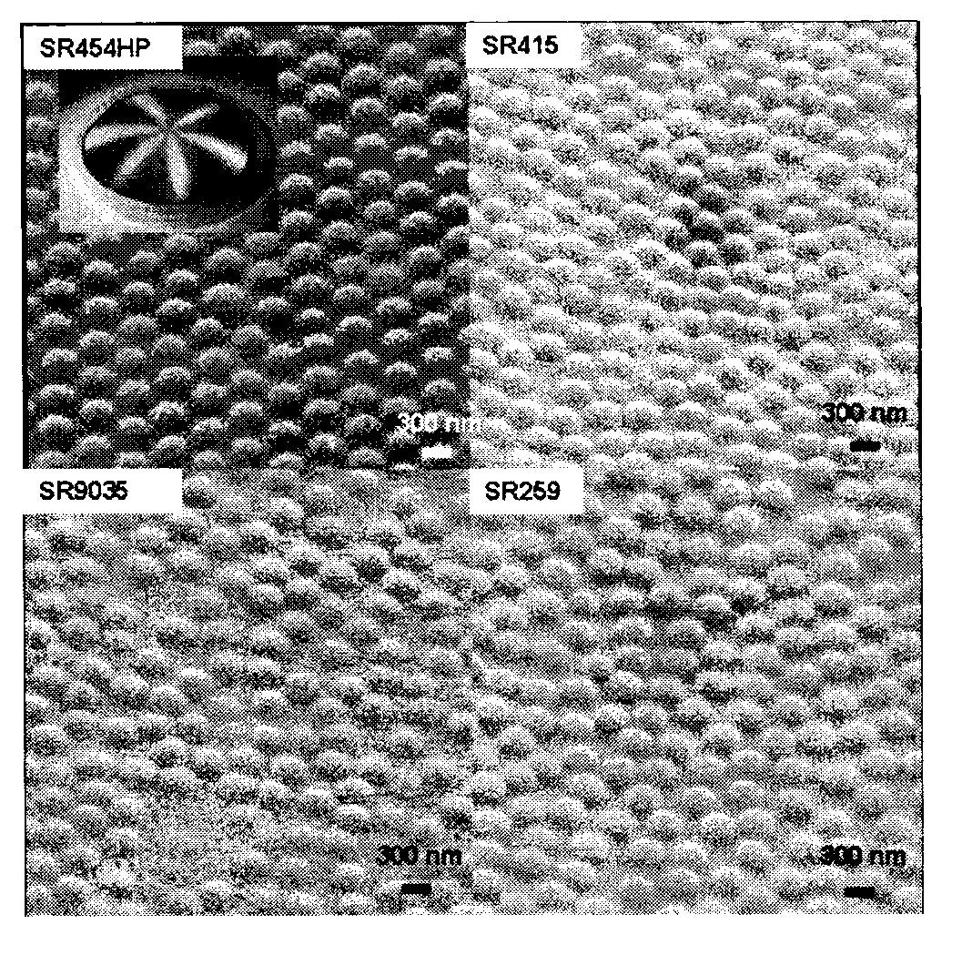
[0017] Silica microspheres with a diameter of 300nm and the polymerizable monomer SR454HP were formulated into a solid-liquid suspension mixture with a volume ratio of 1:4, and the silica-SR454HP solid-liquid suspension mixture was uniformly coated on the diameter of On the surface of a 15.24 cm single crystal silicon wafer, pulse UV light for 12 seconds to initiate in-situ polymerization and solidification of the silica-SR454HP solid-liquid suspension mixture, and then use an electron beam evaporation gold plating equipment to coat a 18nm gold film to prepare nanospheres Convex planar array type SERS substrate. attached figure 1 It is a field emission scanning electron microscope image of a nanosphere convex plane array type SERS substrate, and an electronic digital photo of the obtained SERS substrate is inserted in the figure. The nano-silica microspheres are wra...

Embodiment 2

[0018] Example 2 Preparation and Structural Characterization of Nanosphere Convex Plane Array SERS Substrate

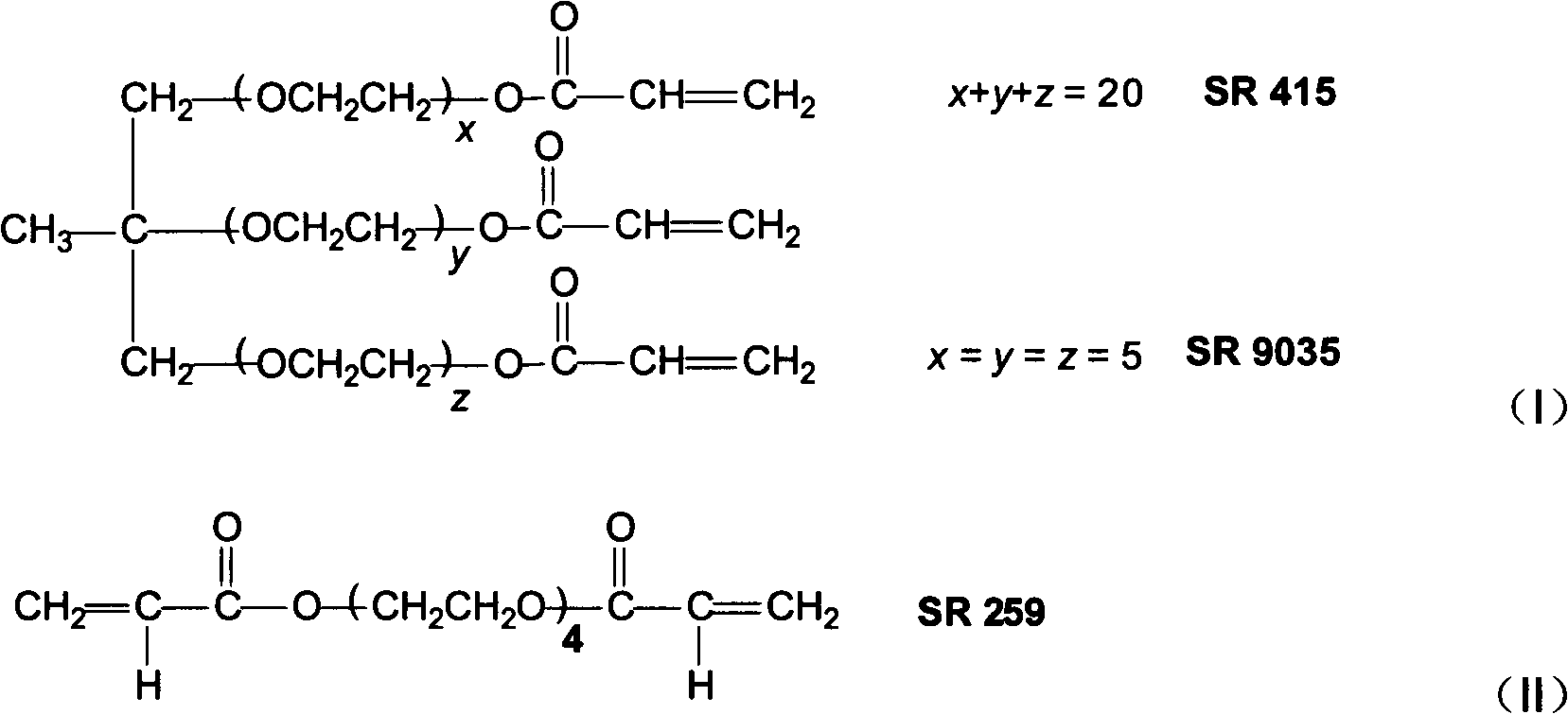
[0019] Silica microspheres with a diameter of 300nm and polymerizable monomer SR415 were formulated into a solid-liquid suspension mixture with a volume ratio of 1:4, and the silica-SR415 solid-liquid suspension mixture was evenly coated on the surface with a diameter of On the surface of a 15.24 cm single crystal silicon wafer, pulse UV light for 12 seconds to initiate in-situ polymerization and solidification of the silica-SR415 solid-liquid suspension mixture, and then use an electron beam evaporation gold plating equipment to coat a 18nm gold film to prepare nanospheres Convex planar array type SERS substrate. From attached figure 1 It can be seen that the arrangement of nano-spherical protrusions is good, and the arrangement density of nano-spherical protrusions on the substrate surface is 6.86×10 8 piece / cm 2 .

Embodiment 3

[0020] Example 3 Preparation and Structural Characterization of Nanosphere Convex Plane Array SERS Substrate

[0021] Silica microspheres with a diameter of 300nm and polymerizable monomer SR9035 were formulated into a solid-liquid suspension mixture with a volume ratio of 1:4, and the silica-SR9035 solid-liquid suspension mixture was uniformly coated on the surface with a diameter of On the surface of a 15.24 cm single crystal silicon wafer, pulse UV light for 12 seconds to initiate in-situ polymerization and solidification of the silica-SR9035 solid-liquid suspension mixture, and then use an electron beam evaporation gold plating equipment to coat a 18nm gold film to prepare nanospheres Convex planar array type SERS substrate. From attached figure 1 It can be seen that the arrangement of nano-spherical protrusions is good, and the arrangement density of nano-spherical protrusions on the substrate surface is 4.52×10 8 piece / cm 2 .


PUM

PropertyMeasurementUnit
diameteraaaaaaaaaa
diameteraaaaaaaaaa

Abstract

The invention discloses a method for regulating the structure of a nanosphere convex plane array type SERS (Surface Enhanced Raman Scattering) substrate, belonging to the field of nanometer material science and technology. According to the method, the regulation on the structure of a nanosphere convex plane array type SERS substrate can be realized by changing the varieties of polymerizable monomers, and the enhanced Raman scattering property of the surface of the nanosphere convex plane array type SERS substrate to laser can be further regulated. The method for regulating structure of the nanosphere convex plane array type SERS substrate has the advantages of being simple in steps, having no environment pollution, being capable of realizing high-flux production and the like.

Description

technical field [0001] The invention relates to a method for adjusting and controlling the nanosphere convex plane array type SERS substrate structure, which belongs to the field of nanomaterial science and technology. Background technique [0002] Surface-enhanced Raman scattering (SERS) is a high-efficiency analytical technique with a sensitivity up to the single-molecule level, and has important application prospects in the fields of chemistry, environment, food, and life sciences. Due to the long-range electromagnetic enhancement and short-range chemical enhancement, the SERS substrate can amplify the weak Raman signal of the measured molecule (adsorbed on the substrate surface) by 10 6 times or greater. Since the commercialization of micro confocal Raman spectrometer, the major breakthroughs in SERS analysis technology are always closely related to the development of SERS substrates. Randomly roughened metal electrodes and random aggregates of colloidal metal particle...

Claims


Application Information

Patent Timeline
Patent Type & Authority Applications(China)
IPC IPC(8): B81C1/00C08F292/00C08F222/20C08F2/48C09D4/02
Inventor 刘雪锋洪清华金美月
Owner JIANGNAN UNIV
Why Eureka
Try Eureka