Wafer detection method and wafer detection apparatus

A detection method and detection device technology, which are applied to measurement devices, optical testing flaws/defects, instruments, etc., can solve the problems of occupying a large space, affecting the detection accuracy, and the volume of the incident light system, etc., so as to reduce the design difficulty, Improve detection efficiency and increase the effect of detection signals

Active Publication Date: 2013-04-03
SKYVERSE TECH CO LTD
View PDF8 Cites 13 Cited by
  • Summary
  • Abstract
  • Description
  • Claims
  • Application Information

AI Technical Summary

Problems solved by technology

The characteristics of large numerical aperture and high resolution obviously put forward high requirements on the optical part of the detection system, which also increases the production cost
[0011] In addition, since each spot is 3 microns x 9 microns in size on the wafer, that is, the spot size is 3 microns in diameter, at a wavelength of 355 nanometers, the numerical aperture of the incident light needs to be between 0.11-0.12. When the DOE is introduced at the same time, the volume of the incident light system will be relatively large and occupy a large space
Due to the limited space, the incident light system has a certain limitation on the numerical aperture of the lighting system, which prevents the lighting system from being close to the surface of the wafer to be tested
The light intensity scattered by particles is mainly concentrated in the solid angle direction of the grazing angle close to the wafer surface, and the limited numerical aperture of lighting will reduce the signal intensity of particle detection, thereby affecting the detection accuracy

Method used


Image

  • Wafer detection method and wafer detection apparatus
  • Wafer detection method and wafer detection apparatus
  • Wafer detection method and wafer detection apparatus

Examples


Embodiment Construction

[0054] In the following description, numerous specific details are set forth in order to provide a thorough understanding of the present invention. However, the present invention can be implemented in many other ways different from those described here, and those skilled in the art can make similar extensions without violating the connotation of the present invention, so the present invention is not limited by the specific implementations disclosed below.

[0055] Secondly, the present invention is described in detail by means of schematic diagrams. When describing the embodiments of the present invention in detail, for convenience of explanation, the schematic diagrams are only examples, which should not limit the protection scope of the present invention.

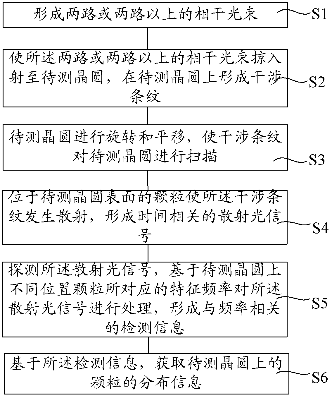
[0056] In order to solve the problems in the prior art, the present invention provides a wafer testing method, comprising: forming two or more coherent beams; making the two or more coherent beams grazing incident on the w...


PUM

PropertyMeasurementUnit
lengthaaaaaaaaaa

Abstract

The invention relates to a wafer detection method and a wafer detection apparatus. The method comprises enabling grazing incidence of two or more than two coherent light beams onto the to-be-measured wafer and forming interference fringes on the to-be-measured wafer; performing rotation and translation for the to-be-measured wafer so that the interference fringes scan the to-be-measured wafer; scattering the interference fringes by particles on the surface of the to-be-measured wafer and forming time-related scattered light signals; detecting the scattered light signals, treating the scattered light signals based on characteristic frequency corresponding to the particles at different positions of the to-be-measured wafer, and forming frequency-dependent detection information; and obtaining the distribution information of the particles on the to-be-measured wafer based on the detection information. The wafer detection method is high in precision and throughput; and the wafer detection apparatus is low in design difficulty and cost.

Description

technical field [0001] The invention relates to the technical field of semiconductors, in particular to a wafer detection method and a wafer detection device. Background technique [0002] In the semiconductor process, the cleanliness of the wafer surface is one of the important factors affecting the reliability of semiconductor devices. How to remove contamination and foreign matter particles on the wafer surface has always been a research hotspot in the field of semiconductor technology, and how to detect the cleanliness of the wafer surface after cleaning has also become a concern of semiconductor technicians. [0003] The optical inspection method has become one of the most commonly used wafer inspection methods due to its advantages of not destroying the cleanliness of the wafer surface and being able to detect in real time. The optical detection method uses optical scattering intensity measurement technology to detect the presence or absence of particles on the wafer ...

Claims


Application Information

Patent Timeline
Patent Type & Authority Applications(China)
IPC IPC(8): G01N21/94
CPCG01N21/9501G01N21/94
Inventor 陈鲁
Owner SKYVERSE TECH CO LTD
Why Eureka
Try Eureka