Memory and memorizing method thereof

A memory, phase change memory technology, applied in static memory, instruments, etc., can solve the problems of low code density and lack of testing flexibility for customers, and achieve the effect of high customer code density, providing quality and stability, and flexible testing.

Active Publication Date: 2013-04-03
SHANGHAI XINCHU INTEGRATED CIRCUIT
View PDF4 Cites 2 Cited by
  • Summary
  • Abstract
  • Description
  • Claims
  • Application Information

AI Technical Summary

Problems solved by technology

[0005] The invention overcomes the defects of lack of test flexibility and low density of customer code in the prior art, and proposes a memory and its storage method

Method used


Image

  • Memory and memorizing method thereof
  • Memory and memorizing method thereof
  • Memory and memorizing method thereof

Examples


Embodiment Construction

[0028] The present invention will be further described in detail in conjunction with the following specific embodiments and accompanying drawings. The process, conditions, experimental methods, etc. for implementing the present invention, except for the content specifically mentioned below, are common knowledge and common knowledge in this field, and the present invention has no special limitation content.

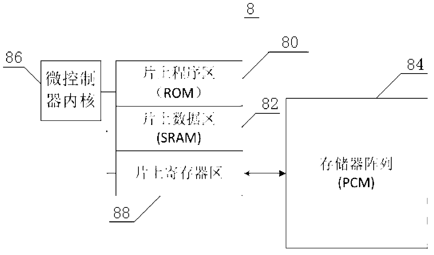
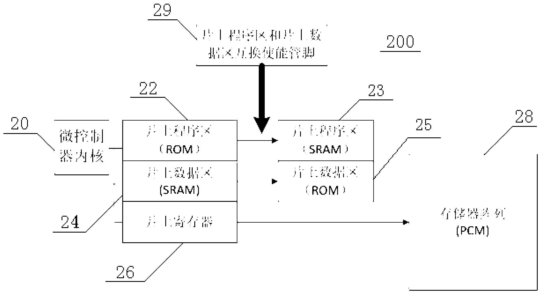
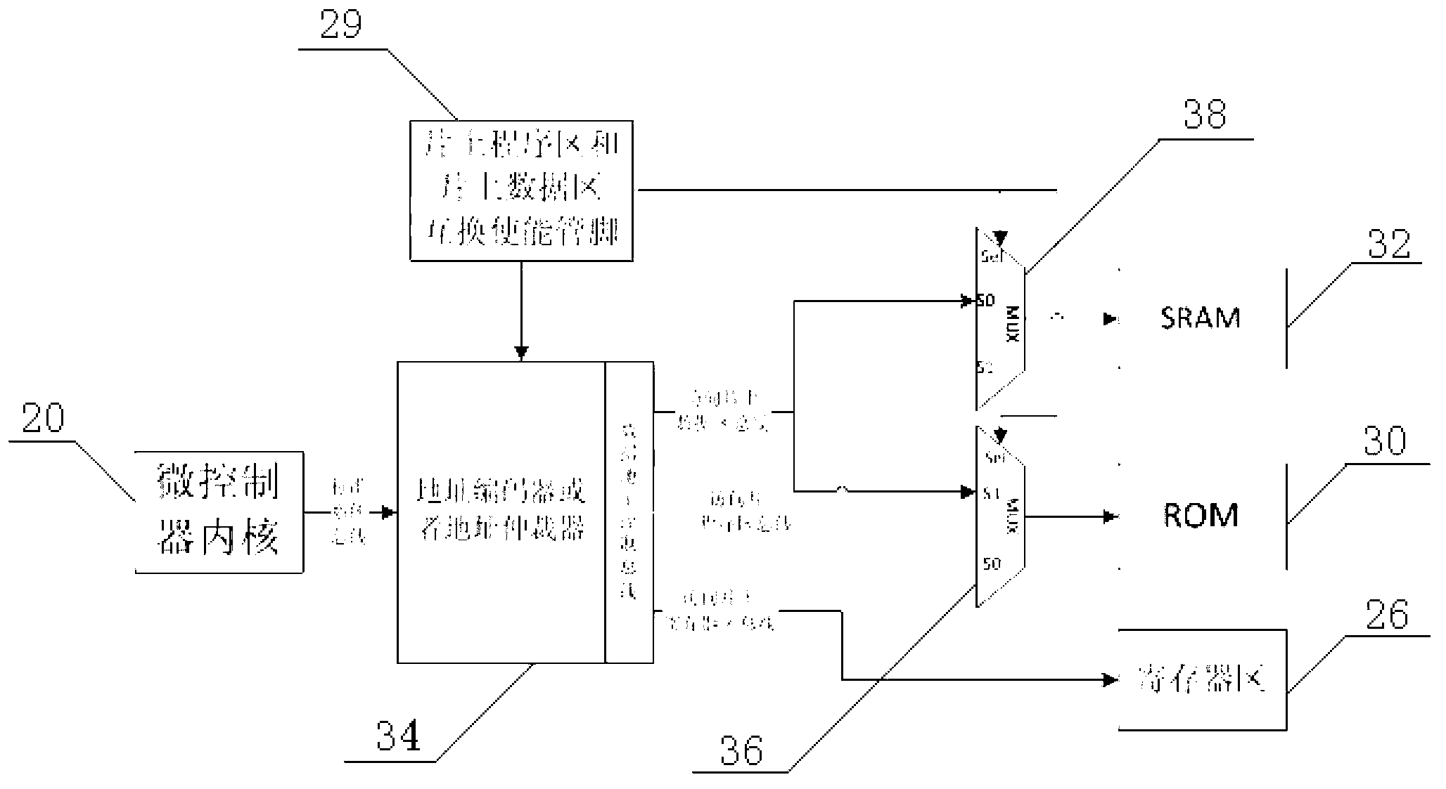
[0029] In the stage of large-scale testing and verification of chips, such as memory, the test factory will download a large number of test codes to the on-chip program area of ​​the chip, and the test code will be executed by the chip core, and the memory array will be directly accessed through the register output to achieve the purpose of testing . The main test contents include Read Window Budget, aging test of phase change memory area, and data retention test. Most of the existing on-chip program areas are ROM or PCM in material selection, but these two configurations...


PUM


Abstract

The invention discloses a memory which comprises an on-chip program area and an on-chip data area that are arranged for a normal working mode, an on-chip program area and on-chip data area exchange enable pin, an on-chip address encoder or an address arbiter module, a first selector, and a second selector, wherein the on-chip program area and on-chip data area exchange enable pin provides an enable signal for exchanging the on-chip program area and the on-chip data area; the on-chip address encoder or the address arbiter module receives the enable signal, and outputs a program area bus accessing to the on-chip program area, and a data area bus accessing to the on-chip data area; the first selector is provided with a selection end for receiving the enable signal, an input end for receiving the program area bus, an input end for receiving the data area bus, and an output end connected with the on-chip program area; and the second selector is provided with a selection end for receiving the enable signal, an input end for receiving the program area bus, an input end for receiving the data area bus, and an output end connected with the on-chip data area. The memory has the advantages of flexible testing, high client code density, and the like. The invention further discloses a memorizing method of the memory.

Description

technical field [0001] The invention relates to the field of chip testing, in particular to a memory and a storage method thereof. Background technique [0002] Phase-change memory testing is a staple of non-volatile flash memory testing. figure 1 It is a schematic structural view of an independent phase-change memory 8; wherein the on-chip program area 80 is realized by a read-only memory (ROM, Read Only Memory), and the on-chip data area 82 is realized by a static random access memory (SRAM, StaticRandom Access Memory) and the memory array 84 is implemented by a phase-change memory (PCM, Phase-Change Memory). Microcontroller core 86 accesses on-chip program area 80 , on-chip data area 82 , and on-chip register area 88 , and accesses on-chip memory array 84 through the output of on-chip register area 88 . [0003] In fact, the reason why the on-chip program area 80 usually uses ROM is because high temperatures will be generated on the chip during packaging and board-level...

Claims


Application Information

Patent Timeline
Patent Type & Authority Applications(China)
IPC IPC(8): G11C29/56
Inventor 景蔚亮
Owner SHANGHAI XINCHU INTEGRATED CIRCUIT
Why Eureka
Try Eureka