Method for preparing graphene image with specific edge

A technology of graphene and graphene film, applied in semiconductor/solid-state device manufacturing, electrical components, circuits, etc., can solve problems such as inconvenience, high cost, and unsuitable for large-scale production and application

Inactive Publication Date: 2013-04-03
SHANGHAI INTEGRATED CIRCUIT RES & DEV CENT
View PDF4 Cites 18 Cited by
  • Summary
  • Abstract
  • Description
  • Claims
  • Application Information

AI Technical Summary

Problems solved by technology

For graphene with only a single layer or a few layers of carbon atoms, it is not convenient to use traditional XRD to determine its crystal orientat

Method used


Image

  • Method for preparing graphene image with specific edge
  • Method for preparing graphene image with specific edge
  • Method for preparing graphene image with specific edge

Examples


Embodiment Construction

[0023] Embodiments embodying the features and advantages of the present invention will be described in detail in the following description. It should be understood that the invention can have various changes in different examples without departing from the scope of the invention, and that the descriptions and illustrations therein are illustrative in nature rather than limiting the invention.

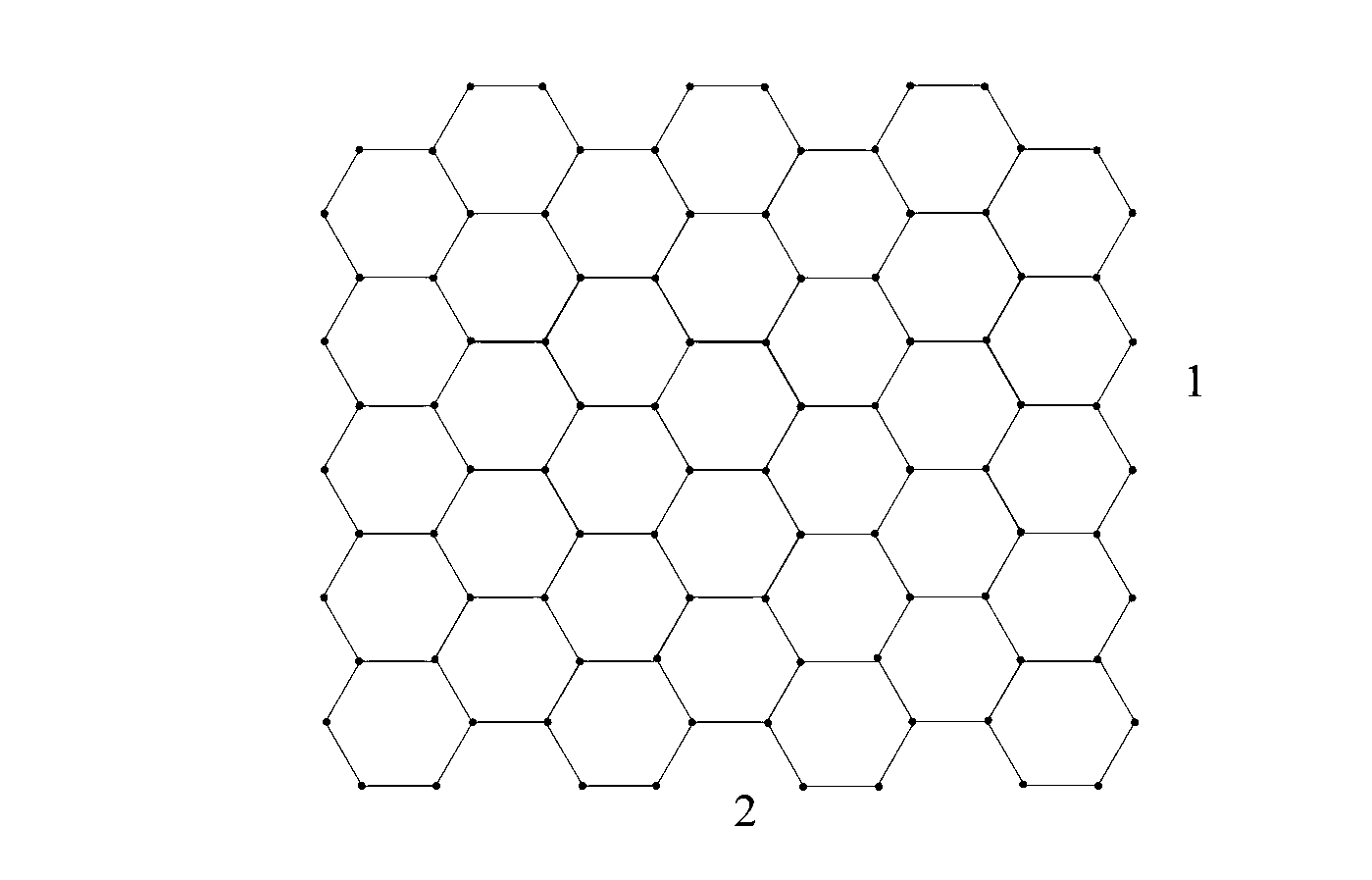
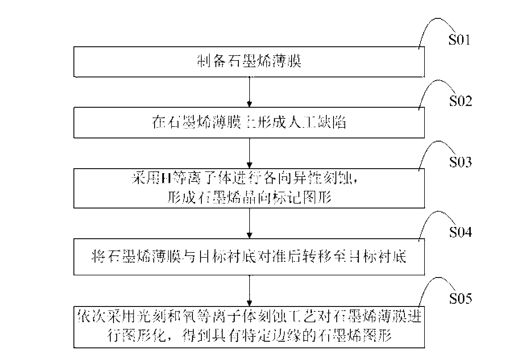
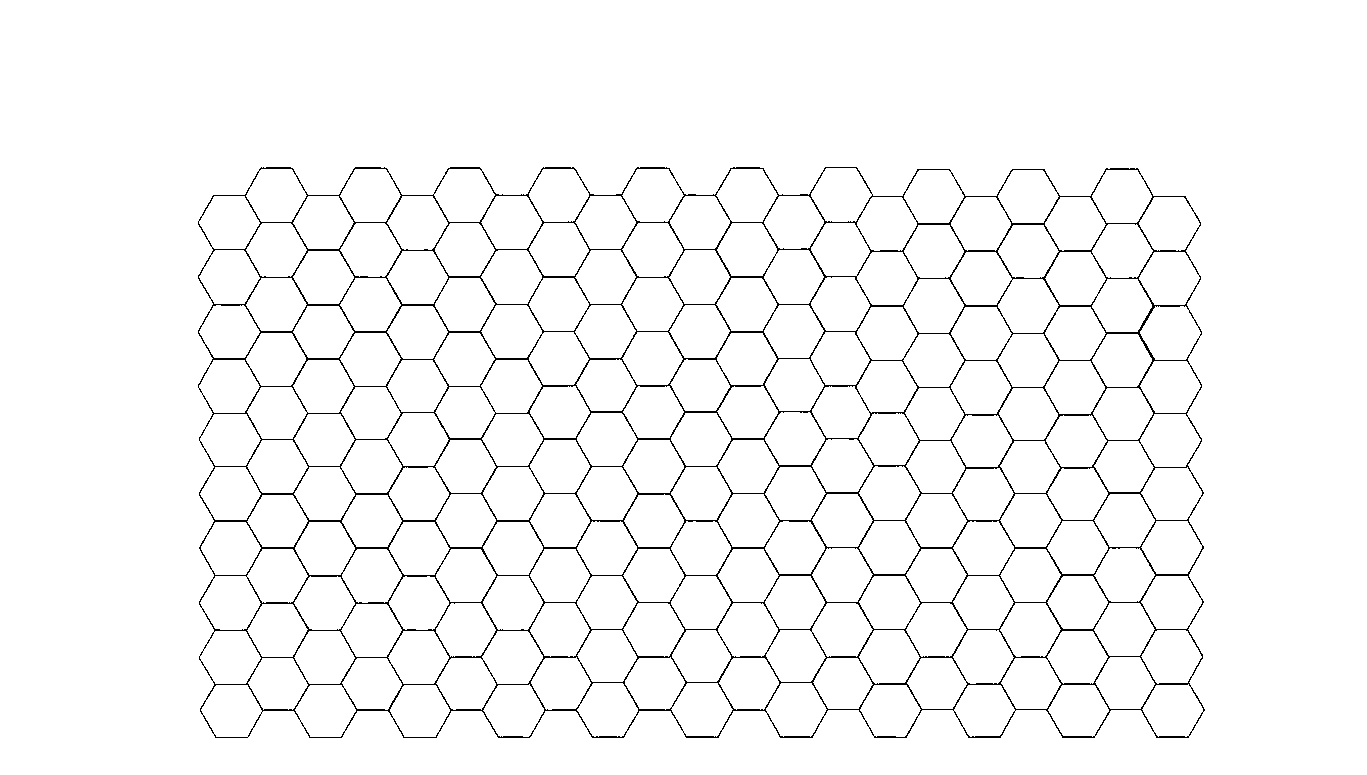
[0024] now attached Figure 2-7 , a method for preparing a graphene pattern with a specific edge in the present invention will be further described in detail through a specific embodiment. It should be noted that all the drawings are in a very simplified form and use imprecise scales, and are only used to facilitate and clearly assist the purpose of illustrating the embodiments of the present invention.

[0025] figure 2 It is a schematic flow chart of a preferred embodiment of a method for preparing graphene graphs with specific edges in the present invention. Figure 3-7 It is a s...


PUM


Abstract

The invention provides a method for preparing a graphene image with a specific edge. The method comprises the steps of preparing a graphene thin film; forming an artificial defect on the graphene thin film; carrying out anisotropic etching on the graphene thin film by H(hydrogen)-containing plasma and forming a graphene crystal orientation mark image along the artificial defect; aligning the graphene thin film with the graphene crystal orientation mark image to a target substrate and transferring the graphene thin film to the target substrate; and imaging the graphene thin film by using a photoetching technology and an oxygen plasma etching technology in sequence, thus obtaining the graphene image with the specific edge. By the method for preparing the graphene image with the specific edge provided by the invention, the image with the specific edge can be prepared and therefore graphene thin films with different properties are obtained; the application of graphene in different fields is facilitated; and the method is simple and compatible with the conventional CMOS (Complementary Metal-Oxide-Semiconductor Transistor) technology, thus being beneficial to popularization application.

Description

technical field [0001] The invention relates to the technical field of integrated circuits, and in particular to a method for preparing graphene graphs with specific edges. Background technique [0002] Graphene is composed of a dense layer of carbon atoms wrapped in a honeycomb crystal lattice. It is the thinnest two-dimensional material in the world, and its thickness is only the thickness of a single atomic layer—on the order of several angstroms. This special structure contains rich and novel physical phenomena, which makes graphene exhibit many excellent properties. For example, the strength of graphene is the highest among the tested materials, reaching 130GPa, more than 100 times that of steel; its carrier mobility reaches 15000cm 2 / (V·s), which is twice that of the currently known indium antimonide material with the highest mobility, and more than 10 times the mobility of commercial silicon wafers. Under certain conditions (such as low temperature quenching, etc.),...

Claims


Application Information

Patent Timeline
IPC IPC(8): H01L21/02
Inventor 左青云康晓旭曾绍海
Owner SHANGHAI INTEGRATED CIRCUIT RES & DEV CENT
Why Eureka
Try Eureka