Check patentability & draft patents in minutes with Patsnap Eureka AI!

A wafer pre-alignment device

A pre-alignment, wafer technology, applied in electrical components, semiconductor/solid-state device manufacturing, circuits, etc., can solve the problems of increased positioning time, low device efficiency, waste of space, etc., to improve positioning accuracy and compact mechanism design. , the effect of improving the detection efficiency

Active Publication Date: 2015-08-26
SHANGHAI JIAO TONG UNIV
View PDF5 Cites 0 Cited by
  • Summary
  • Abstract
  • Description
  • Claims
  • Application Information

AI Technical Summary

Problems solved by technology

As we all know, the thickness of the wafer itself is about 0.7mm, and local deformation will occur during vacuum adsorption. This deformation will have an adverse effect on the entire pre-alignment result and directly affect the positioning accuracy, because the wafer The edge scanning on the table and the centroid is calculated from the scanning data, and then the wafer is transferred to the horizontal centering unit by vacuum handover for centering, and finally the centered wafer is transferred to the wafer table again Orientation of the gap, this method causes two superimpositions of error data, and also increases the positioning time, making the efficiency of the device low
At the same time, because the device uses ball screw splines for transmission, and the linear array CCD sensor detects the edge signal of the wafer, the size of the entire device is too large, wasting a lot of space

Method used


Image

  • A wafer pre-alignment device
  • A wafer pre-alignment device
  • A wafer pre-alignment device

Examples


Embodiment Construction

[0047] The present invention will be described in detail below in conjunction with specific embodiments. The following examples will help those skilled in the art to further understand the present invention, but do not limit the present invention in any form. It should be noted that those skilled in the art can make several modifications and improvements without departing from the concept of the present invention. These all belong to the protection scope of the present invention.

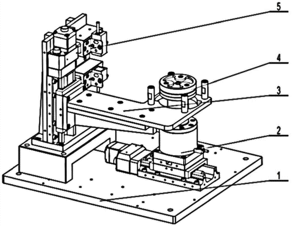
[0048] Such as figure 1 As shown, in this embodiment, the wafer pre-alignment device provided by the present invention includes a worktable 1, a θ-Y two-degree-of-freedom motion unit 2, a vertical transition unit 3, a vacuum adsorption unit 4, a visual inspection unit 5 and Data acquisition unit and motion control unit not marked on the above. The θ-Y two-degree-of-freedom motion unit 2 is used to adjust the eccentricity and notch position of the wafer, and is fixed on the worktable 1; the vertic...


PUM


Abstract

The invention provides a wafer prealignment device. The wafer prealignment device comprises a working table, a theta-Y two-degree-of-freedom movement unit, a perpendicular transition unit, a vacuum absorption unit and a visual inspection unit, wherein the theta-Y two-degree-of-freedom movement unit is used for adjusting eccentricity and a notch position of a wafer; the perpendicular transition unit is used for holding the wafer temporarily to enable the wafer to be completely isolated from the theta-Y two-degree-of-freedom movement unit so that the eccentricity is adjusted; the vacuum absorption unit is coaxially fixed on the theta-Y two-degree-of-freedom movement unit and is used for fixing the wafer to enable the wafer to achieve centering and notch positioning; and the visual inspection unit is used for detecting the edge position and the notch position of the wafer. The designed wafer prealignment device is capable of rotating the maximum radial displacement eccentricity of the wafer to an axis, and accordingly one X-direction degree of freedom can be omitted effectively, one linear movement platform is omitted for the wafer prealignment device, and cost is saved while positioning efficiency is improved.

Description

technical field [0001] The invention relates to a semiconductor manufacturing device, in particular to a wafer pre-alignment device. Background technique [0002] The wafer pre-alignment device is an important subsystem of the wafer processing system. Its function is to position the wafer before the wafer is transferred to the processing station, calculate the deviation of the wafer from the standard position, and then drive the motion platform Position the center of the wafer and the notch (or cut edge) within a specific range. There are two purposes of wafer pre-alignment, one is to determine the position of the center of the wafer, and the other is to determine the direction of the wafer notch. The position of the wafer center on the pre-alignment system is unknown before operation, and the notch direction is also random. The purpose of pre-alignment is to adjust the wafer center to the specified position and the notch direction to the specified direction. [0003] The ...

Claims


Application Information

Patent Timeline
IPC IPC(8): H01L21/68
Inventor 张波刘品宽朱晓博张帆梁家欣
Owner SHANGHAI JIAO TONG UNIV
Features
  • R&D
  • Intellectual Property
  • Life Sciences
  • Materials
  • Tech Scout
  • Unparalleled Data Quality
  • Higher Quality Content
  • 60% Fewer Hallucinations
Learn More