Preparation method of conductive plastic with ordered space network structure
A network structure, conductive plastic technology, used in cable/conductor manufacturing, circuits, electrical components, etc., can solve problems such as cost increase and composite material performance degradation, and achieve the effect of improving product performance, low filling amount, and expanding the scope of use
- Summary
- Abstract
- Description
- Claims
- Application Information
AI Technical Summary
Problems solved by technology
Method used
Image

Examples
Embodiment 1
[0021] First, mix 7 grams of specific conductive carbon black (SCB), 7 grams of processing aids, and 700 grams of polyethylene (PE) particles with a high-speed mixer for 3 minutes; then put 714 grams of the mixed particles into the micro-nano particle shaping bag Coating system, processing at 5000rpm for 8 minutes, and discharging for 2 minutes; finally, the composite particles were hot-pressed at 210°C and 14Mpa for 30 minutes to obtain a conductive plastic with an ordered spatial conductive network structure.
Embodiment 2
[0023] First, mix 21 grams of specific conductive carbon black (SCB), 5 grams of processing aids, and 700 grams of polyethylene (PE) particles with a high-speed mixer for 3 minutes; then put 726 grams of the mixed particles into the micro-nano particle shaping bag Coating system, processing at 5000rpm for 8 minutes, and discharging for 2 minutes; finally, the composite particles were hot-pressed at 210°C and 14Mpa for 30 minutes to obtain a conductive plastic with an ordered spatial conductive network structure.
Embodiment 3
[0025] First, mix 35 grams of specific conductive carbon black (SCB), 3 grams of processing aids, and 700 grams of polyethylene (PE) particles with a high-speed mixer for 3 minutes; then put 738 grams of the mixed particles into the micro-nano particle shaping bag Coating system, processing at 5000rpm for 8 minutes, and discharging for 2 minutes; finally, the composite particles were hot-pressed at 210°C and 14Mpa for 30 minutes to obtain a conductive plastic with an ordered spatial conductive network structure.
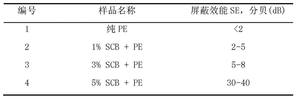
[0026] The electromagnetic shielding properties of the prepared conductive plastics with an ordered spatial conductive network structure are shown in Table 1.
[0027] Table 1 SCB filling amount and shielding effectiveness range
[0028]
PUM
 Abstract
Description
Claims
Application Information