Silicon material with nano-structure surface and manufacturing method thereof

A technology of nanostructures and manufacturing methods, which is applied in the fields of technology for producing decorative surface effects, microstructure technology, microstructure devices, etc., and can solve the problems of inability to complete nanoparticles, inability to realize nanocolumnar surface silicon structures, and inability to obtain silicon nanostructures. Columnar structure and other issues, to achieve the effects of easy promotion and application, mature etching process, and strong process adaptability

Inactive Publication Date: 2013-04-10
INST OF HIGH ENERGY PHYSICS CHINESE ACADEMY OF SCI
View PDF9 Cites 10 Cited by
  • Summary
  • Abstract
  • Description
  • Claims
  • Application Information

AI Technical Summary

Problems solved by technology

Due to the characteristics and mechanism limitations of metal nano-film technology, the diameter of metal self-assembled nanoparticles produced generally does not exceed 100 nanometers, so it is impossible to complete nanoparticles with a diameter of several hundred to microns, and it is also impossible to obtain silicon nano-columnar structures at this scale.
However, the wet-etched porous silicon structure can only complete the pore structure of various diameters, and cannot realize the silicon structure on the nano-columnar surface.

Method used


Image

  • Silicon material with nano-structure surface and manufacturing method thereof
  • Silicon material with nano-structure surface and manufacturing method thereof
  • Silicon material with nano-structure surface and manufacturing method thereof

Examples


Embodiment

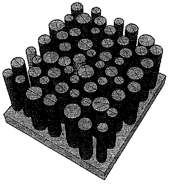
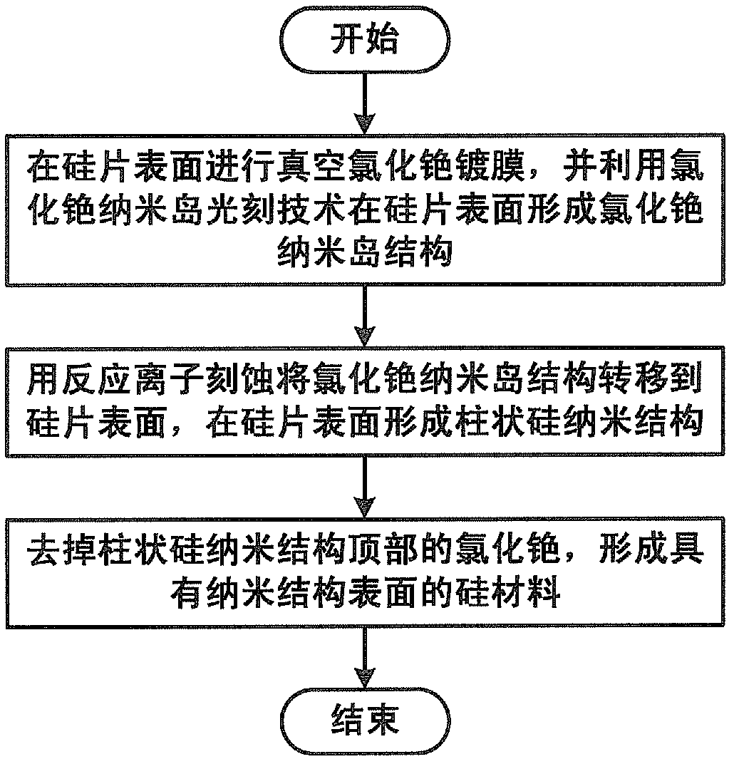
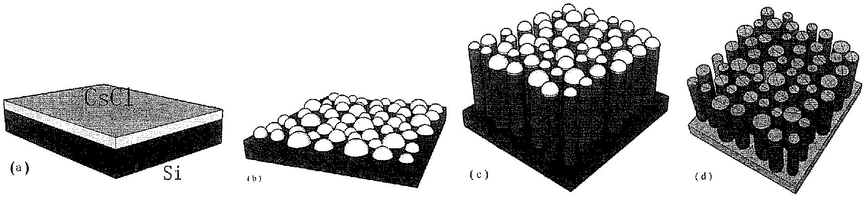
[0030] Evaporate a cesium chloride film on a silicon wafer with a thermal evaporation method, and the film thickness is 100 nanometers. Thickness is measured and controlled with a quartz crystal thickness gauge. Put the silicon wafer coated with cesium chloride film into a ventilated cavity with a humidity of 40%, the humidity is controlled by the flow of humid gas flowing into the cavity, and develop for 1 hour under this humidity condition, so that the cesium chloride film is agglomerated into a The nano-island structure forms a cesium chloride nano-island structure on the surface of the silicon wafer. The cesium chloride nano-islands have an average diameter of 400 nm. Put the silicon wafer with cesium chloride island structure on the surface into the etching chamber of the reactive ion etching machine, the etching process parameters are pressure 5Pa, etching gas, and etching time 10 minutes. The silicon chip is taken out and placed in water for 5 minutes to dissolve the ...


PUM

PropertyMeasurementUnit
Thicknessaaaaaaaaaa

Abstract

The invention discloses a silicon material with a nano-structure surface and a manufacturing method thereof. The silicon material comprises a silicon wafer with a certain thickness, and a columnar silicon nano-structure formed by the condition that the surface of the silicon wafer is etched. The method comprises the following steps: carrying out vacuum cesium chloride film coating on the surface of the silicon wafer; forming a cesium chloride nano island structure on the surface of the silicon wafer by utilizing a cesium chloride nano island photetching technology; transferring the cesium chloride nano island structure to the surface of the silicon wafer by utilizing reaction icon etching; forming the columnar silicon nano-structure on the surface of the silicon wafer; and removing the cesium chloride on the top of the columnar silicon nano-structure, so as to form the silicon material with the nano-structure surface. With the adoption of the silicon material with the nano-structure surface and the manufacturing method thereof, an original nano structure is finished by adopting a cesium chloride nano island self-assembling technology; the silicon material with the nano-structure surface and the manufacturing method are low in cost and stronger in process adaptability, can grow and finish on different silicon surfaces, and are beneficial for popularization and application.

Description

technical field [0001] The invention relates to the technical field of micron / nano semiconductor micromachining, in particular to a silicon material with a nanostructured surface and a manufacturing method thereof. Background technique [0002] Silicon is one of the most versatile semiconductor materials, with huge industrial applications in solar cells and many other fields. At present, the fabrication of nanostructures on silicon surfaces mainly includes nano-island structures self-assembled by metal thin film technology and porous silicon nanopore structures by wet etching. Such as utilizing the high-temperature magnetically controlled silver process to obtain silver nanostructures, and then using reactive ion etching to convert the silver nanostructures into nano-silicon columnar structures, the process method is basically the same as that of the present invention, except that reactive ion etching uses The mask structure is silver nanostructure. Due to the characterist...

Claims


Application Information

Patent Timeline
IPC IPC(8): B81C1/00
Inventor 伊福廷
Owner INST OF HIGH ENERGY PHYSICS CHINESE ACADEMY OF SCI
Why Eureka
Try Eureka