Process for producing semiconductor

A manufacturing process and semiconductor technology, applied in semiconductor devices, semiconductor/solid-state device manufacturing, electrical components, etc., can solve problems such as poor quality, reduced electrical quality of semiconductor structures, and uneven surfaces

Active Publication Date: 2013-04-10
UNITED MICROELECTRONICS CORP
View PDF4 Cites 7 Cited by
  • Summary
  • Abstract
  • Description
  • Claims
  • Application Information

AI Technical Summary

Problems solved by technology

However, the sidewalls of the fin structure formed by the etching photolithography process have uneven surfaces and many defects caused by etching, resulting in poor quality channel regions and subsequent vias to be formed thereon cannot be obtained. Tight coverage, thereby degrading the electrical quality of the semiconductor structures formed thereon

Method used


Image

  • Process for producing semiconductor
  • Process for producing semiconductor
  • Process for producing semiconductor

Examples


Embodiment Construction

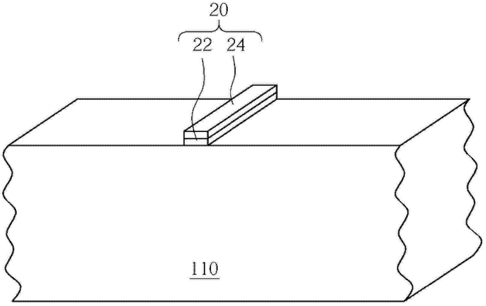
[0030] Figure 1-Figure 10 A schematic cross-sectional view of a semiconductor fabrication process according to an embodiment of the present invention is shown. Such as figure 1 As shown, a base 110 is provided, and the base 110 in this embodiment is a monolithic base. Certainly, the substrate 110 may include a silicon substrate, a silicon-containing substrate, a group III-V silicon-on-silicon substrate (such as GaN-on-silicon), a graphene-on-silicon substrate (graphene-on-silicon), or a silicon-on-insulator substrate. and other semiconductor substrates. Next, a mask layer 20 is formed on the substrate 110 , wherein the mask layer 20 may include a pad oxide layer 22 and a nitride layer 24 on the pad oxide layer 22 . Then, an etching and photolithography process is performed to pattern the mask layer 20 and expose part of the substrate 110 .

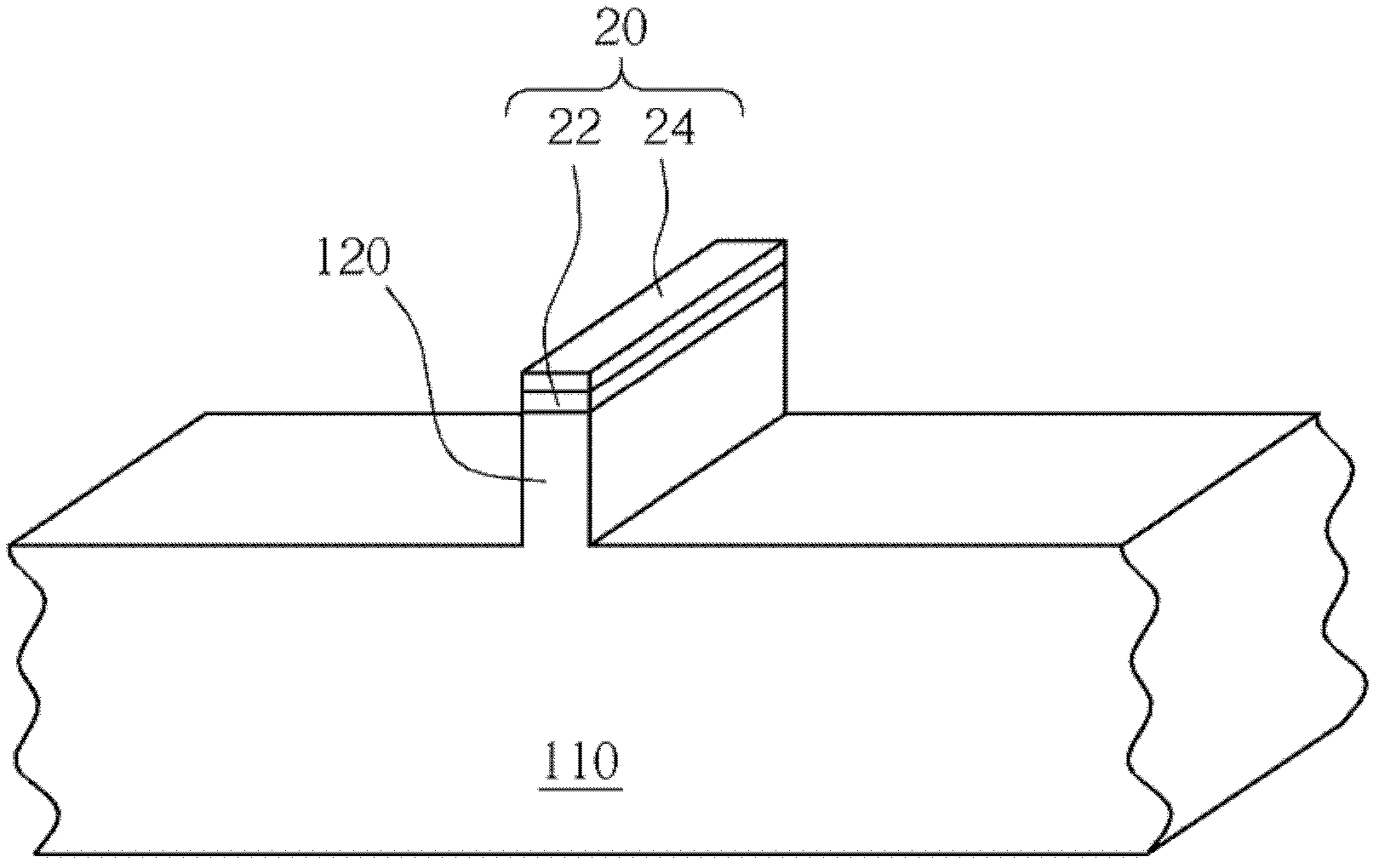
[0031] Such as figure 2 As shown, the substrate 110 is etched using the mask layer 20 as a hard mask to form a fin structure 120 ...


PUM


Abstract

The invention discloses a process for producing a semiconductor. The method comprises steps of providing a substrate, forming at least one fin-shaped structure on the substrate and an oxide layer on the position of the substrate, which is except the fin-shaped structure, conducting a heat treatment production process and enabling the side wall of part of the fin-shaped structure to form a melted layer.

Description

technical field [0001] The invention relates to a semiconductor manufacturing process, in particular to a semiconductor manufacturing process which adopts a heat treatment manufacturing process to make the side wall of a fin structure more flat. Background technique [0002] As the size of semiconductor devices shrinks, maintaining the performance of small-sized semiconductor devices is a major goal of the industry. In order to improve the performance of semiconductor devices, various Fin-shaped field effect transistors (FinFETs) have been gradually developed. FinFET devices include the following advantages. First of all, the manufacturing process of fin field effect transistor elements can be integrated with the traditional logic element manufacturing process, so it has considerable manufacturing process compatibility; secondly, due to the three-dimensional shape of the fin structure, the contact between the gate and the single crystal silicon is increased. Area, so it ca...

Claims


Application Information

Patent Timeline
Patent Type & Authority Applications(China)
IPC IPC(8): H01L21/324H01L21/28H01L21/336
CPCH01L29/66795H01L29/7854
Inventor 林建良蔡世鸿林俊贤孙德霖王韶韦颜英伟王俞仁
Owner UNITED MICROELECTRONICS CORP
Why Eureka
Try Eureka