Manufacture method for insulated gate bipolar transistor (IGBT) device

A manufacturing method and device technology, applied in semiconductor/solid-state device manufacturing, electrical components, circuits, etc., can solve problems such as fragmentation incidents, increased warpage of silicon wafers, and inability to tape out silicon wafers, so as to solve transmission problems and improve The effect of warpage

Inactive Publication Date: 2013-04-10
SHANGHAI HUAHONG GRACE SEMICON MFG CORP
View PDF8 Cites 4 Cited by
  • Summary
  • Abstract
  • Description
  • Claims
  • Application Information

AI Technical Summary

Problems solved by technology

However, since the IGBT separation device requires a very thick metal layer, when the production of the IGBT separation device enters the final metal layer deposition, the backside process is not performed before the final metal layer is deposited. After the final metal layer is deposited, the thick metal layer will produce very Due to the large normal stress, no matter how the previous process steps improve the radius of curvature after trench gate deposition, the stress deterioration of the thick metal layer cannot be overcome. Severe stress will lead to an increase in the warpage of the silicon wafer, making subsequent metal layer photolithography Difficulties in handling with the etching process, which may even lead to failure of silicon wafer tape-out or occurrence of debris events (see figure 1 shown)

Method used


Image

  • Manufacture method for insulated gate bipolar transistor (IGBT) device
  • Manufacture method for insulated gate bipolar transistor (IGBT) device
  • Manufacture method for insulated gate bipolar transistor (IGBT) device

Examples


Embodiment Construction

[0017] In one embodiment of the present invention, the manufacturing method of the IGBT device includes the following steps:

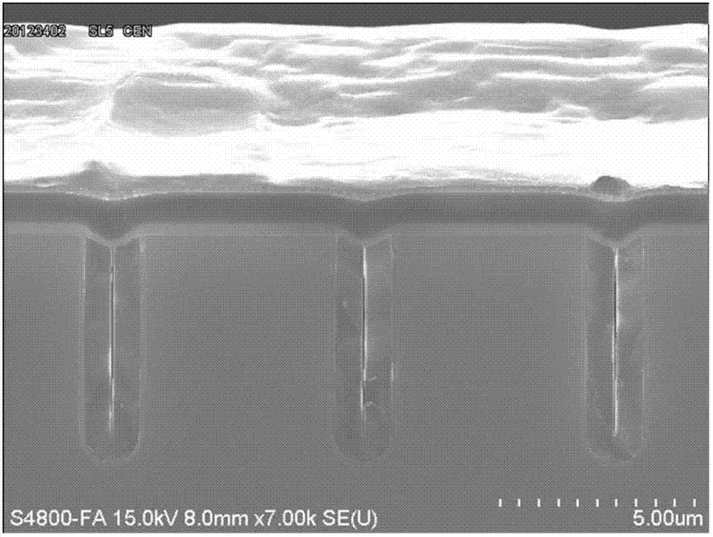
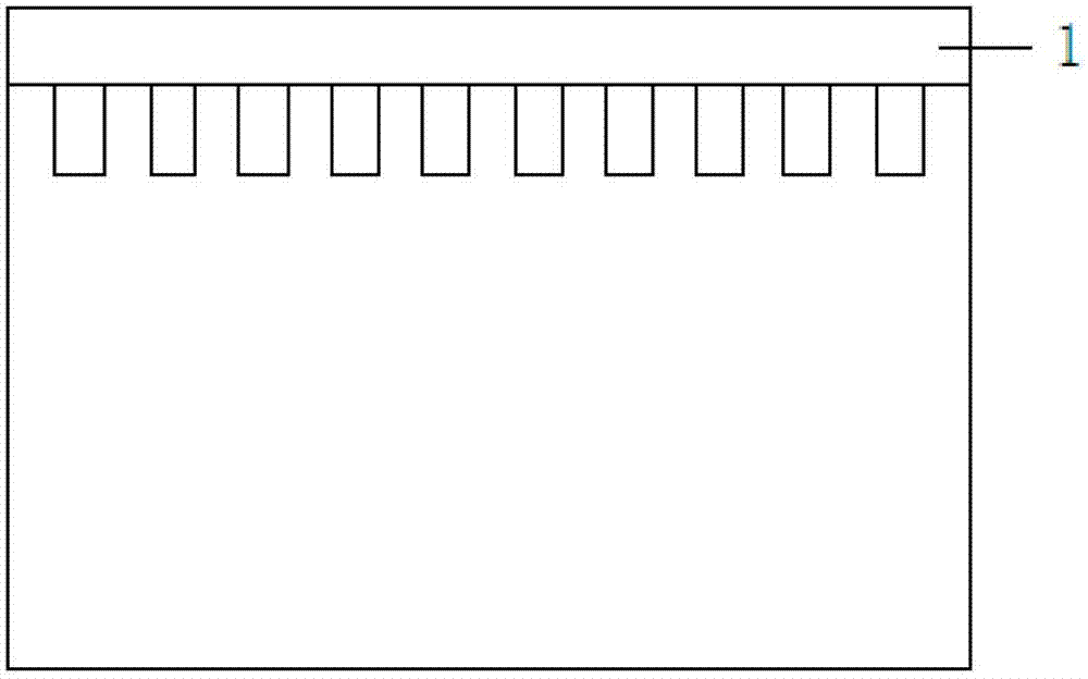
[0018] first step, combine figure 2 As shown, trench etching is performed sequentially on the silicon wafer for making IGBT separation devices, a gate oxide layer is formed in the trench, and then the trench is filled with polysilicon (ie, gate polysilicon). A pre-metal dielectric layer 1 is deposited on the upper end surface of the silicon wafer (that is, the front side of the silicon wafer) of the part structure of the IGBT separation device that has been formed.

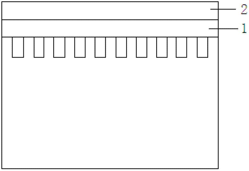
[0019] Step two, combine image 3 As shown, a protective film 2 is deposited on the upper end of the pre-metal dielectric layer 1, and the protective film 2 can effectively prevent possible scratches on the front surface of the device during subsequent back process steps. The protective film 2 is generally an atmospheric pressure CVD (chemical vapor deposition) film, or a film of other ...


PUM


Abstract

The invention discloses a manufacture method for an insulated gate bipolar transistor (IGBT) device. Before a metal layer of an IGBT separation device deposits, a film with positive stress is formed at the back of a silicone wafer of a formed device structure. The manufacture method can effectively offset stress of the metal layer, improves warping degree of the silicon wafer and enables follow-up photoetching and etching on the metal layer to be constructed normally.

Description

technical field [0001] The invention relates to the field of semiconductor integrated circuits, in particular to a method for manufacturing a low-stress IGBT (insulated gate bipolar transistor) device. Background technique [0002] In various semiconductor device structures, trench thyristors are widely used in various power devices due to their special channel characteristics and electrical characteristics. Especially for IGBT devices, due to its unique high-voltage and high-current working environment, its trench IGBT devices require larger-sized trench gates. With the improvement of device performance requirements by end customers, the trench required by the device is getting deeper and deeper, and the stress of the trench gate is becoming more and more prominent. [0003] The radius of curvature of each step in the manufacturing process of IGBT devices is shown in Table 1. [0004] Process steps Wafer radius of curvature (m) Shot 332 tr...

Claims


Application Information

Patent Timeline
Patent Type & Authority Applications(China)
IPC IPC(8): H01L21/331H01L21/31
Inventor 成鑫华李琳松季伟李刚
Owner SHANGHAI HUAHONG GRACE SEMICON MFG CORP
Why Eureka
Try Eureka