Method for producing electronic device
A technology of electronic devices and manufacturing methods, applied in the direction of lamination devices, chemical instruments and methods, circuits, etc., to achieve the effect of excellent productivity
- Summary
- Abstract
- Description
- Claims
- Application Information
AI Technical Summary
Problems solved by technology
Method used
Image

Examples
no. 1 Embodiment approach ]
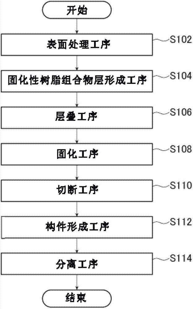
[0070] figure 1 It is a flowchart showing the manufacturing process in one embodiment of the manufacturing method of the electronic device of the present invention. Such as figure 1 As shown, the manufacturing method of an electronic device includes a surface treatment step S102, a curable resin composition layer forming step S104, a lamination step S106, a curing step S108, a cutting step S110, a member forming step S112, and a separation step S114.
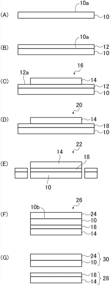
[0071] in addition, figure 2 It is a schematic cross-sectional view sequentially showing each manufacturing process in the manufacturing method of the electronic device of this invention.
[0072] Below, refer to figure 2 The materials used in each process and their order are described in detail. First, the surface treatment step S102 will be described in detail.
[0073] [Surface treatment process]
[0074] The surface treatment step S102 is a step of treating the first main surface of the glass substrate having the f...
no. 2 Embodiment approach ]
[0221] Figure 7 It is a flowchart showing the manufacturing process in another embodiment of the manufacturing method of the electronic device of this invention. Such as Figure 7 As shown, the manufacturing method of an electronic device includes a surface treatment step S102, a curable resin composition layer forming step S104, a lamination step S106, a defoaming step S116, a curing step S108, a cutting step S110, a member forming step S112, and a separation step S114 .
[0222] Figure 7 In addition to the point that each process shown in has the defoaming process S116, it is the same as figure 1 The steps shown in are in the same order, and the same reference numerals are assigned to the same steps, and the description thereof will be omitted, and the defoaming step S116 will be mainly described below.
[0223] [Degassing process]
[0224] The defoaming process S116 is a process of performing defoaming treatment of the uncured curable resin composition layer after t...
Embodiment 1)
[0230] A glass substrate used as a peelable glass substrate is cleaned with pure water or UV to clean its surface. Thereafter, a mask was applied to the second main surface which is one side of the glass substrate, and then a heptane solution having a silicone oil content of 1% by mass was sprayed on the opposite first main surface and dried. Silicone oil uses dimethyl polysiloxane (manufactured by DowCorning Corporation, SH200, kinematic viscosity 190~210mm 2 / s). Next, heat processing was performed at 350 degreeC for 5 minutes in order to reduce the molecular weight of a silicone oil, and the peelable glass substrate was obtained.
[0231] Then, when the water contact angle of the first main surface of the peelable glass substrate was measured using a contact angle meter (manufactured by KRUSS, DROP SHAPEANALYSIS SYSTEM DSA 10Mk2), it was 100°.
[0232] In addition, the first main surface of the peelable glass substrate was measured using an atomic force microscope (manufa...
PUM
| Property | Measurement | Unit |
|---|---|---|
| Kinematic viscosity | aaaaa | aaaaa |
| Surface roughness | aaaaa | aaaaa |
| Thickness | aaaaa | aaaaa |
Abstract
Description
Claims
Application Information