Piezoresistive strain gauge with ceramic substrate
A ceramic substrate and ceramic substrate technology, applied in the field of strain gauges, can solve the problems of short life, easy aging, poor stability, etc., and achieve the effects of low cost, good insulation, and small creep
- Summary
- Abstract
- Description
- Claims
- Application Information
AI Technical Summary
Problems solved by technology
Method used
Image

Examples
Embodiment 1
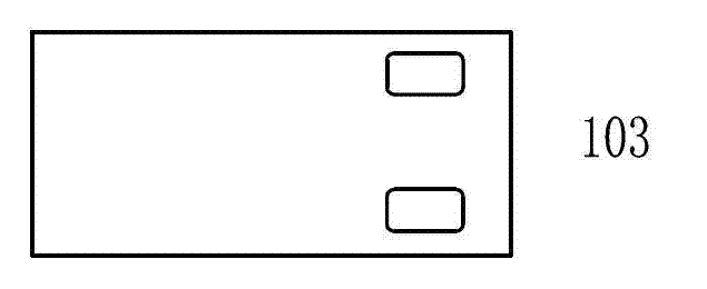
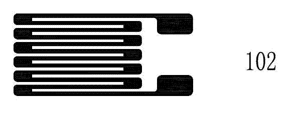
[0043] Figure 7 ~ Figure 13 It is a schematic diagram of Embodiment 1 of the present invention. This embodiment is a strain gauge with a single resistance, which is suitable for applications such as load cells.
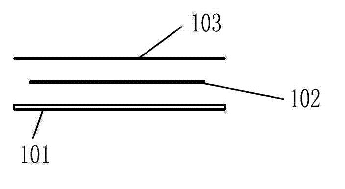
[0044] Such as Figure 7 ~ Figure 13 As shown, the upper surface of the ceramic substrate 301 is printed and sintered to form a conductor layer 302, a thick film resistance layer 303, and an insulating protective layer 304, and then the sealing glass paste is printed on the lower surface of the ceramic substrate 301, dried or Sintering forms the sealing glass layer 305 . The ceramic substrate 301 is made of an alumina ceramic sheet with a thickness of about 0.1 mm. The conductive layer 302 is made of gold paste with a film thickness of about 1-5 microns. The thick-film resistance layer 303 is a single resistance, and the ruthenium-based resistance paste with a square resistance coefficient of 10KΩ is selected, and the film thickness is 5-10 microns. The insulatin...
Embodiment 2
[0046] Figure 14 ~ Figure 20 It is a schematic diagram of Embodiment 2 of the present invention. This embodiment consists of four resistors to form a Wheatstone bridge, which is a full-bridge strain gauge and is mainly used for pressure sensors.
[0047] Such as Figure 14 ~ Figure 20 As shown, similar to Embodiment 1, the upper surface of the ceramic substrate 401 is printed and sintered to form a conductor layer 402, a thick film resistance layer 403, and an insulating protective layer 404, and then the sealing glass paste is printed on the lower surface of the ceramic substrate 401. material, dried or sintered to form the sealing glass layer 405. The difference from the first embodiment is that, in the second embodiment, the thick film resistor layer 403 is a Wheatstone bridge composed of four resistors.
[0048] To sum up, the present invention uses ceramics as the base material. Ceramics have the characteristics of corrosion resistance, high temperature resistance, low...
PUM
| Property | Measurement | Unit |
|---|---|---|
| thickness | aaaaa | aaaaa |
| thickness | aaaaa | aaaaa |
| thickness | aaaaa | aaaaa |
Abstract
Description
Claims
Application Information