Low-power dissipation static random access memory (SRAM) type field programmable gate array (FPGA) design method

A design method and low power consumption technology, applied in the direction of logic circuits using specific components, logic circuits using basic logic circuit components, etc., to achieve the effects of reduced read and write power consumption, good anti-interference ability, and reduced power consumption

Inactive Publication Date: 2013-04-24
SOUTHEAST UNIV
View PDF6 Cites 5 Cited by
  • Summary
  • Abstract
  • Description
  • Claims
  • Application Information

AI Technical Summary

Problems solved by technology

Although the current mainstream SRAM-based FPGA is more and more integrated and its technology is more and more advanced, because its leakage current is equal to or even exceeds the working current of FPGA with the improvement of technology, it has become a bottleneck for FPGA to achieve low power consumption.

Method used


Image

  • Low-power dissipation static random access memory (SRAM) type field programmable gate array (FPGA) design method
  • Low-power dissipation static random access memory (SRAM) type field programmable gate array (FPGA) design method
  • Low-power dissipation static random access memory (SRAM) type field programmable gate array (FPGA) design method

Examples


Embodiment Construction

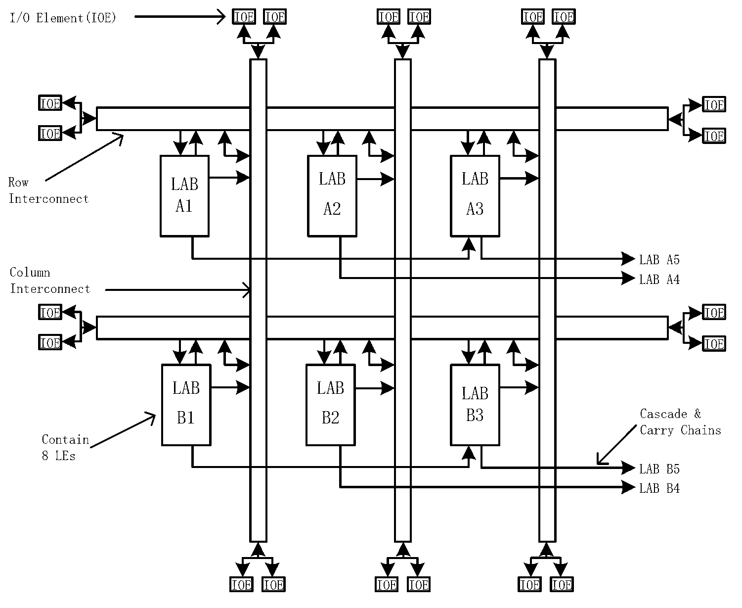
[0018] Although the structure of FPGA, CPLD and other types of PLD has its own characteristics and strengths, in general, they are composed of three major parts, such as figure 1 As shown, it includes:

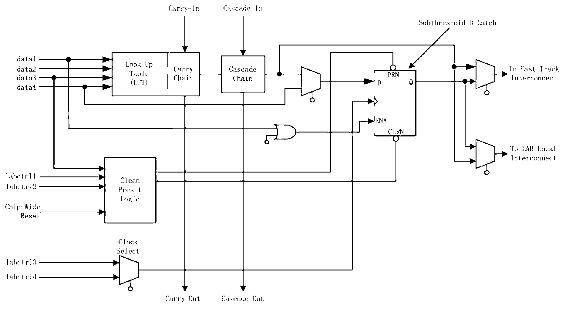
[0019] (1) A two-dimensional logic block array LAB constitutes the logic composition core of the SRAM type FPGA, and each LAB is composed of 8 logic units LE (Logic Element), and LE is the circuit to be discussed in the present invention. figure 1 The cascade and carry chain signals in LE are also derived from LE, see figure 2 ;

[0020] (2) Input / output block IOE (I / O Element);

[0021] (3) The interconnection resources connecting the logic blocks are composed of wire segments of various lengths, and there are also some programmable connection switches, which are used for the connection between logic blocks, between logic blocks and input and output blocks.

[0022] Logic unit LE is the smallest logic unit in FPGA, which can effectively implement logic functions. Each LA...


PUM


Abstract

Provided is a low-power dissipation static random access memory (SRAM) type field programmable gate array (FPGA) design method. A level shifter is used for at least reducing working voltage of a two-dimensional logical block array of the FPGA to a near-threshold, the Schmidt trigger type SRAM is adopted in a look up table (LUT) in the two-dimensional logical block array, a sub-threshold D latch is adopted in a programmable D-flip flop, the LUT and the programmable D-flip flop work under reduced low supply voltage, and therefore the FPGA works normally under ultra-low supply voltage. The invention provides the novel method. According to the method, the level shifter is used for reducing the working voltage of the two-dimensional logical block array of the FPGA to be in a near-threshold or even a sub-threshold area, the FPGA can work normally under the ultra-low supply voltage, and therefore the FPGA can further achieve work of ultra-low power dissipation.

Description

technical field [0001] The invention belongs to the technical field of integrated circuits, relates to a field programmable gate array FPGA, in particular to a low-power FPGA working under the condition of an ultra-low power supply voltage, and is a design method of a low-power SRAM FPGA. Background technique [0002] FPGA (Field Programmable Gate Array), that is, Field Programmable Gate Array, is a product of further development on the basis of programmable devices such as PAL, GAL, and CPLD. It appears as a semi-custom circuit in the field of application-specific integrated circuits (ASIC), which not only solves the shortcomings of custom circuits, but also overcomes the shortcomings of the limited number of gate circuits of original programmable devices, and makes it fast to market and low design cost. They play an increasingly important role in the field of complex logic circuits and digital signal processing. Among them, SRAM-type FPGA has received more and more favors...

Claims


Application Information

Patent Timeline
Patent Type & Authority Applications(China)
IPC IPC(8): H03K19/177
Inventor 刘波柏娜陈愿
Owner SOUTHEAST UNIV
Why Eureka
Try Eureka