Process method for processing titanium nitride residues on aluminum welding pad

A process method, titanium nitride technology, applied in the direction of electrical components, semiconductor/solid-state device manufacturing, circuits, etc.

Active Publication Date: 2013-05-01
SHANGHAI HUALI MICROELECTRONICS CORP
View PDF4 Cites 8 Cited by
  • Summary
  • Abstract
  • Description
  • Claims
  • Application Information

AI Technical Summary

Problems solved by technology

It is used to solve the problem that titanium nitride residues will be produced when aluminum metal is etched in the prior art, and these residual titanium nitrides will cause the problem that the quality of subsequent metal welding wires will be affected after welding

Method used


Image

  • Process method for processing titanium nitride residues on aluminum welding pad
  • Process method for processing titanium nitride residues on aluminum welding pad
  • Process method for processing titanium nitride residues on aluminum welding pad

Examples


Embodiment Construction

[0029] In order to make the technical means, creative features, objectives and effects of the invention easy to understand, the present invention will be further elaborated below in conjunction with specific diagrams.

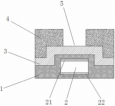
[0030] Such as Figure 3A As shown, in a specific embodiment of the present invention, a process method for treating titanium nitride residues on an aluminum pad includes: a substrate 1, a metal layer 2 provided in the substrate 1, a substrate 1 and a metal layer A top metal barrier layer 21 is provided between the upper surface of the layer 2, a bottom metal barrier layer 22 is provided between the substrate 1 and the lower surface of the metal layer 2, a barrier layer 3 is provided on the upper surface of the substrate 1, and the barrier layer 3 is deposited. The photoresist layer 4, the photoresist layer 4 is located directly above the metal layer 2 and hollowed out 5, which includes the following process steps:

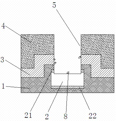
[0031] Such as Figure 3B As shown, in ste...


PUM


Abstract

The invention provides a process method for processing titanium nitride residues on an aluminum welding pad. The process method comprises the following steps of: step 1, etching a barrier layer which is not covered by a photoresist layer, a substrate below the barrier layer and a top metal barrier layer until a metal layer is etched; step 2, completely removing the photoresist layer; step 3, depositing silicon nitride; covering the silicon nitride on the barrier layer, the top of a side wall of the substrate, a side wall of the metal barrier layer and the upper surface of the metal layer; step 4, carrying out photoresist layer deposition on the upper surface of the metal layer; utilizing a condition of aluminum welding pad photoetching to carry out coating and developing of light resistance; step 5, etching the silicon nitride which is not covered by the photoresist layer; step 6, removing the photoresist layer; and step 7, carrying out chemical washing. According to the process method for processing the titanium nitride residues on the aluminum welding pad disclosed by the invention, under the precondition of keeping the appearance of the aluminum welding pad, the titanium nitride residues on the aluminum welding pad can be removed and overmuch loss of bottom aluminum is not caused; and meanwhile, the caused waste of wafers can be greatly avoided, the process is simple and extra equipment and materials do not need to be added.

Description

Technical field [0001] The invention involves a residual removal process, especially the process method of treating titanium nitride residues on aluminum welding pads. Background technique [0002] The aluminum welding pad in the rear section is the last semiconductor manufacturing process before the chip is packaged. After the wafer is etching, the final test (appearance testing, electrical test, good rate test) will be entered.Dao packaging phase.Stacking structure of aluminum welding pads figure 1 It is shown that the aluminum is generally aluminum, titanium nitride, silicon oxide, and silicon nitrine. Because the aluminum pads are thick, the height of the wafer surface is uneven, so the insulator blocking layer (silicon oxide and silicon nitride) is relatively thick.Silicon nitride also has the effect of anti -ray and water vapor; because aluminum welding pads are used for subsequent metal welding cables, the areas to be carved are relatively large, generally the tens of micr...

Claims


Application Information

Patent Timeline
Patent Type & Authority Applications(China)
IPC IPC(8): H01L21/02
Inventor 杨渝书李程陈玉文
Owner SHANGHAI HUALI MICROELECTRONICS CORP
Why Eureka
Try Eureka