Laterally diffused metal oxide semiconductor (LDMOS) transistor and formation method thereof
A transistor and semiconductor technology, applied in the fields of semiconductor devices, semiconductor/solid-state device manufacturing, electrical components, etc., can solve the problems of complex process and large area of LDMOS transistors, and achieve the effect of increasing difficulty, large safe working range and reducing internal consumption.
- Summary
- Abstract
- Description
- Claims
- Application Information
AI Technical Summary
Problems solved by technology
Method used
Image
Examples
Embodiment 1
[0056] In this embodiment, an N-type LDMOS transistor is formed as an example (that is, the first conductivity type is P-type, and the second conductivity type is N-type), and the method for forming the LDMOS transistor of the present invention is described.
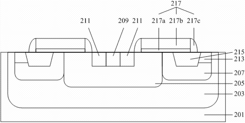
[0057] refer to image 3 Firstly, a semiconductor substrate 201 is provided, and a P-type well region 203 is formed in the semiconductor substrate 201; then, a P-type heavily doped region 205 is formed in the well region 203, and a P-type heavily doped region 205 is formed in the heavily An N-type drift region 207 is formed in the well region 203 on both sides of the doped region 205; then, a shallow trench isolation structure 215 is formed in the drift region 207, and the shallow trench isolation structure 215 is located close to the heavily doped In the drift region 207 on one side of the region 205; then, a gate structure 217 is formed on the semiconductor substrate 201, and the gate structure 217 covers part of the h...
Embodiment 2
[0109] This embodiment takes forming a P-type LDMOS transistor as an example (that is, the first conductivity type is N-type, and the second conductivity type is P-type) to describe the method for forming the LDMOS transistor of the present invention.
[0110] refer to Figure 14 Firstly, a semiconductor substrate 301 is provided, and an N-type well region 303 is formed in the semiconductor substrate 301; then, an N-type heavily doped region 305 is formed in the well region 303, and an N-type well region 305 is formed in the heavily doped region 303; A P-type drift region 307 is formed in the well region 303 on both sides of the doped region 305; then, a shallow trench isolation structure 315 is formed in the drift region 307, and the shallow trench isolation structure 315 is located close to the heavily doped In the drift region 307 on one side of the region 305; then, a gate structure 307 is formed on the semiconductor substrate 301, and the gate structure 307 covers part of...
PUM
 Abstract
Description
Claims
Application Information


