Display device, array substrate and manufacture method of array substrate

An array substrate and substrate technology, applied in the field of display devices, can solve problems such as poor uniformity of common voltage, achieve the effects of reducing the resistance value of common electrodes, improving screen performance, and reducing production costs

Active Publication Date: 2013-05-01
BOE TECH GRP CO LTD
View PDF4 Cites 29 Cited by
  • Summary
  • Abstract
  • Description
  • Claims
  • Application Information

AI Technical Summary

Problems solved by technology

[0007] The technical problem to be solved by the present invention is to provide a display device, an array substrate and a manufacturing method thereof, so as to overcome the green defect caused by the poor uniformity of the common voltage in the existing array substrate

Method used


Image

  • Display device, array substrate and manufacture method of array substrate
  • Display device, array substrate and manufacture method of array substrate
  • Display device, array substrate and manufacture method of array substrate

Examples


Embodiment Construction

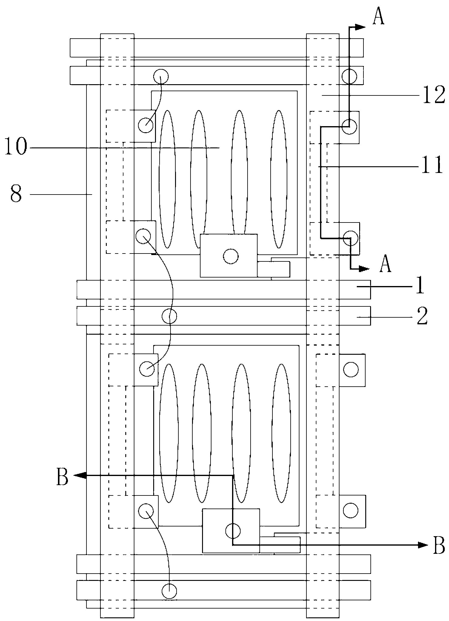
[0042] Embodiments of the present invention are described in detail below, examples of which are shown in the drawings, wherein the same or similar reference numerals designate the same or similar elements or elements having the same or similar functions throughout. The embodiments described below by referring to the figures are exemplary only for explaining the present invention and should not be construed as limiting the present invention.

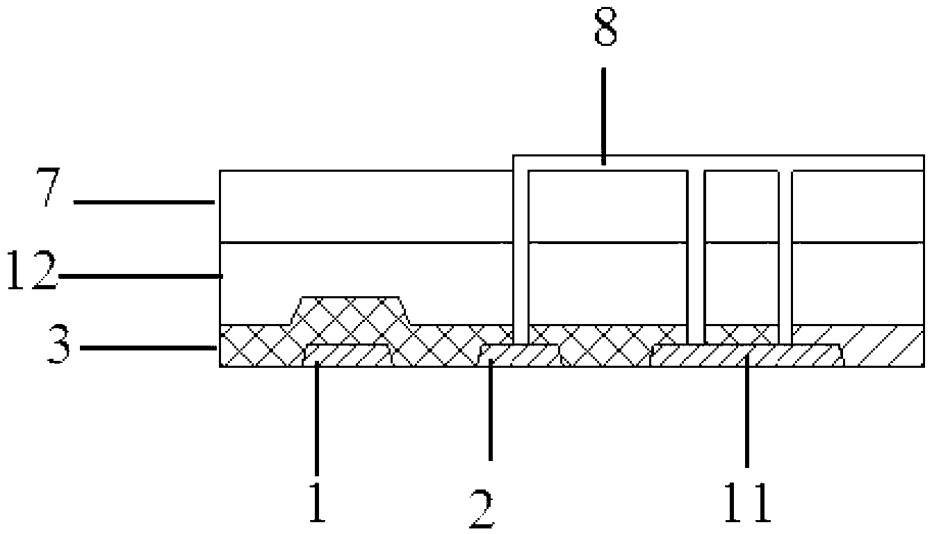
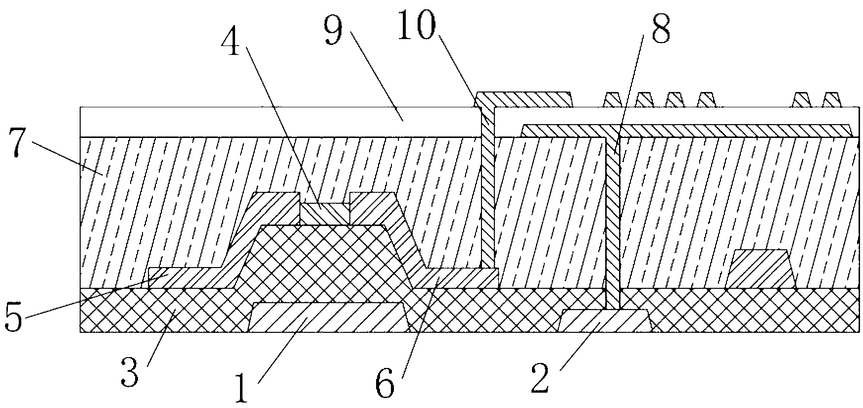
[0043] Such as Figure 1 to Figure 3 As shown, the embodiment of the present invention provides an array substrate, including: a substrate, a plurality of gate lines 1 disposed on the substrate and data lines 12 intersecting the gate lines, and a plurality of horizontal common electrode lines 2 and a plurality of The vertical common electrode lines 11 are located below the data lines 12 , and the horizontal common electrode lines 2 are electrically connected to the vertical common electrode lines 11 .

[0044] Wherein, the horizontal co...


PUM


Abstract

The invention relates to the technical field of display and particularly relates to a display device, an array substrate and a manufacture method of the array substrate. The array substrate comprises a substrate, a plurality of grid wires and data wires, wherein the grid wires are arranged on the substrate, and the grid wires and the data wires are arranged in an intersecting manner. The array substrate further comprises a plurality of transverse common electrode wires and a plurality of longitudinal common electrode wires, wherein the longitudinal common electrode wires are located below the data wires, and the transverse common electrode wires and the longitudinal common electrode wires are electrically connected. According to the display device, the array substrate and the manufacture method of the array substrate, provided by the invention, through arranging the longitudinal common electrode wires below the data wires, common electrodes in the longitudinal direction are extensively connected, and the overall resistance of the common electrodes is decreased, so that a pixel structure is optimized, and the frame performance of a product is maximally improved. Meanwhile, compared with the prior art, the use of a mask patterning process can be reduced, the production efficiency is increased, and the production cost is reduced.

Description

technical field [0001] The present invention relates to the field of display technology, in particular to a display device, an array substrate and a manufacturing method thereof. Background technique [0002] With the development of science and technology, flat-panel displays have replaced bulky CRT displays and are increasingly embedded in people's daily lives. Currently, commonly used flat panel displays include LCD (Liquid Crystal Display, liquid crystal display) and OLED (Organic Light-Emitting Diode, organic light-emitting diode) displays. During the imaging process, each liquid crystal pixel in the LCD display is driven by a thin film transistor (Thin Film Transistor, TFT) integrated in the TFT array substrate, and cooperates with the peripheral driving circuit to realize image display. [0003] In ADS mode, two layers of transparent electrodes (which can be made of indium tin oxide ITO) are formed on the array substrate. Usually, one layer of ITO electrodes is used a...

Claims


Application Information

Patent Timeline
Patent Type & Authority Applications(China)
IPC IPC(8): H01L27/02H01L21/77
Inventor 崔贤植李会徐智强严允晟
Owner BOE TECH GRP CO LTD
Why Eureka
Try Eureka