
Method of improving planarization of surface of shallow trench isolation silicon oxide film

A technology for surface planarization and silicon oxide film, which is used in electrical components, semiconductor/solid-state device manufacturing, circuits, etc., and can solve the limitations of process flexibility, limited help for surface planarization of silicon oxide film, and poor planarization effect, etc. problems to achieve the effect of increasing flexibility

Inactive Publication Date: 2013-05-15
SHANGHAI HUAHONG GRACE SEMICON MFG CORP
View PDF2 Cites 0 Cited by
  • Summary
  • Abstract
  • Description
  • Claims
  • Application Information

AI Technical Summary

Problems solved by technology

[0004] However, the traditional reverse mask process (such as figure 1 shown), there are certain requirements for the mask alignment accuracy, especially in figure 1 In the place marked by the dotted line in the middle, left or right deviation will lead to poor flattening effect
In addition, for reverse mask etching, if only half of SiO is etched 2 If the silicon oxide film surface planarization is limited; etch to Si 3 N 4 If this is the case, the flexibility of the process is limited, that is, it cannot be flexibly adjusted according to different products

Method used


Image

  • Method of improving planarization of surface of shallow trench isolation silicon oxide film
  • Method of improving planarization of surface of shallow trench isolation silicon oxide film
  • Method of improving planarization of surface of shallow trench isolation silicon oxide film

Examples


Embodiment Construction

[0022] The method for improving the surface planarization of shallow trench isolation silicon oxide film of the present invention, its process diagram is as follows figure 2 As shown, the steps include:

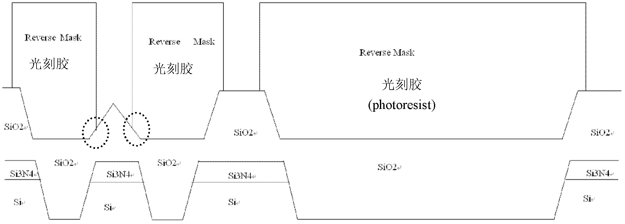
[0023] (1) According to the existing STI process flow, after silicon oxide and silicon nitride deposition on the silicon substrate, STI silicon groove etching, HDP silicon oxide filling (filling), and then after STI CMP, carry out Lithography that opens in AA-dense regions (such as image 3 As shown), in the photolithography process, the thickness of the photoresist is about 1 μm, and the I-line photolithography machine is used for exposure;

[0024] Among them, the AA-intensive area can be: within any range of 10 μm×10 μm inside the chip, the area occupied by AA exceeds 40% or more of the total area;

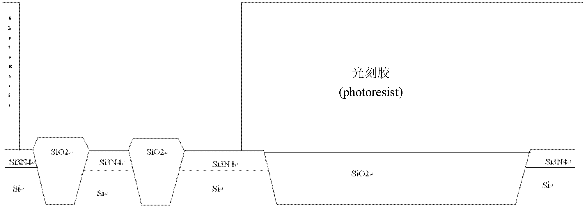
[0025] (2) Use SiO with a high selectivity ratio (greater than 10:1) to silicon nitride for a fixed time 2 Wet etching or dry etching, such as Figure 4 As shown, making ...


PUM


Abstract

The invention discloses a method of improving planarization of surface of a shallow trench isolation silicon oxide film. The method of improving the planarization of surface of the shallow trench isolation silicon oxide film includes the following steps of with regard to silicon oxide filling a shallow trench, lapping the silicon oxide by means of chemical machinery of shallow trench isolation (STI) at first, and then etching the silicon oxide of an active area (AA) compact zone by means of mask, thereby improving the planarization of surface of the shallow trench isolation silicon oxide film. The method of improving the planarization of surface of the shallow trench isolation silicon oxide film can greatly lower requirements to photoetching registration precision, and for instance, a requirement of original 0.1 micrometer is relaxed up to 0.3 micrometer. Due to the fact that etching quantity is reduced, applying a wet etching technology with higher selectivity can be considered. In addition, the method of improving the planarization of surface of the shallow trench isolation silicon oxide film can increase flexibility of the technology, namely, the method of improving the planarization of surface of the shallow trench isolation silicon oxide film can adjust etching time according to different products so as to independently adjust the height of the silicon oxide of the shallow trench isolation in AA compact zone within a certain range (such as + / - 5000A).

Description

technical field [0001] The invention relates to a method for flattening the surface of a shallow trench isolation silicon oxide film, in particular to a method for improving the surface planarization of a shallow trench isolation silicon oxide film. Background technique [0002] In the semiconductor manufacturing process, the shallow trench isolation (Shallow Trench Isolation, STI) process has the advantages of good isolation effect and small footprint. The typical STI process includes: silicon oxide (pad oxide) and nitride on the silicon substrate Silicon deposition, STI silicon groove etching, silicon oxide (HDP Oxide) filling, silicon oxide chemical mechanical polishing (CMP), silicon nitride and silicon oxide (pad oxide) removal. [0003] During the manufacturing process of shallow trench isolation (STI), CMP process is used to remove and planarize over-filled high-density plasma silicon oxide (HDP oxide). Due to the dishing and erosion effects of CMP, the traditional m...

Claims


Application Information

Patent Timeline
IPC IPC(8): H01L21/762H01L21/3105
Inventor 刘俊
Owner SHANGHAI HUAHONG GRACE SEMICON MFG CORP
Features
  • Generate Ideas
  • Intellectual Property
  • Life Sciences
  • Materials
  • Tech Scout
  • Unparalleled Data Quality
  • Higher Quality Content
  • 60% Fewer Hallucinations
Learn More