Wafer back face thinning method

A backside thinning and wafer technology, applied in electrical components, semiconductor/solid-state device manufacturing, circuits, etc., can solve problems such as excessive thickness, increased internal stress, and slow thinning rate, so as to reduce the probability of fragmentation and increase the number of finished products rate, reducing the effect of internal stress

Inactive Publication Date: 2013-05-22
WUHAN XINXIN SEMICON MFG CO LTD
View PDF3 Cites 8 Cited by
  • Summary
  • Abstract
  • Description
  • Claims
  • Application Information

AI Technical Summary

Problems solved by technology

Grinding and thinning speed is fast, which is good for productivity improvement, but grinding is easy to cause wafer cracks, increase internal stress, and the difference in surface thickness is obvious, so it is easy to cause wafer fragments in the subsequent process
Wet etching thinning can relieve the internal stress caused by grinding, and can make the surface have better thickness uniformity, but the thinning rate is slow
At present, the commonly used process for thinning device wafers is to perform one grinding after bonding the device wafer to the carrier, and then perform multiple wet etching. Although this process method utilizes wet etching to a certain extent However, due to the excessive thickness of the grinding, the generated internal stress is correspondingly too large, and device wafer fragments will still occur during the thinning process, which will affect the device wafer yield and cause cost loss

Method used


Image

  • Wafer back face thinning method
  • Wafer back face thinning method
  • Wafer back face thinning method

Examples


Embodiment Construction

[0027] The principles and features of the present invention are described below in conjunction with the accompanying drawings, and the examples given are only used to explain the present invention, and are not intended to limit the scope of the present invention.

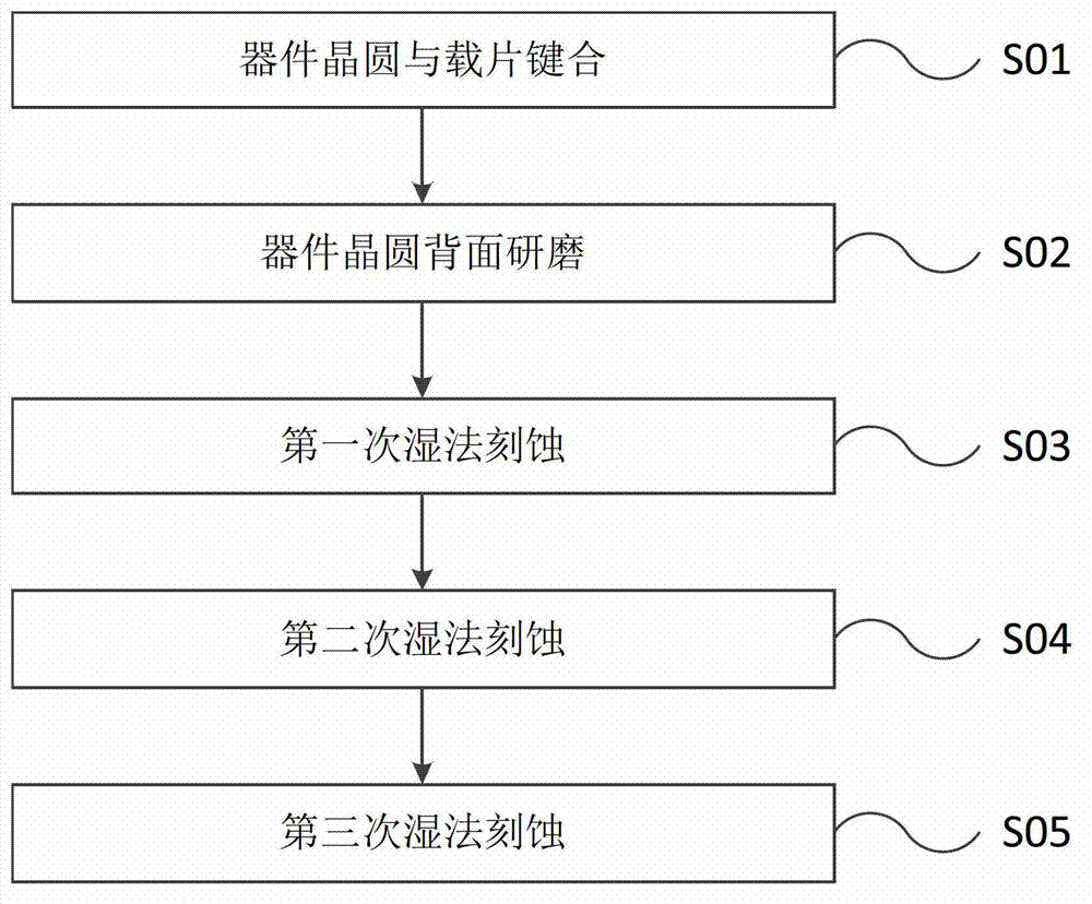
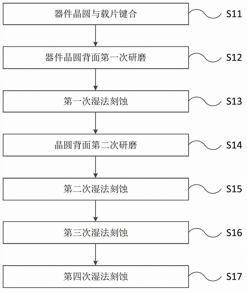
[0028] Such as figure 2 Shown is the prior art process flow chart, comprises the following steps:

[0029] Step S01, bonding the device wafer to the carrier;

[0030] Step S02, performing a second grinding on the back of the device wafer, and grinding the thickness of the device wafer to 50um-25um;

[0031] Step S03, performing a second wet etching on the device wafer, and etching the device wafer to 8um-6um;

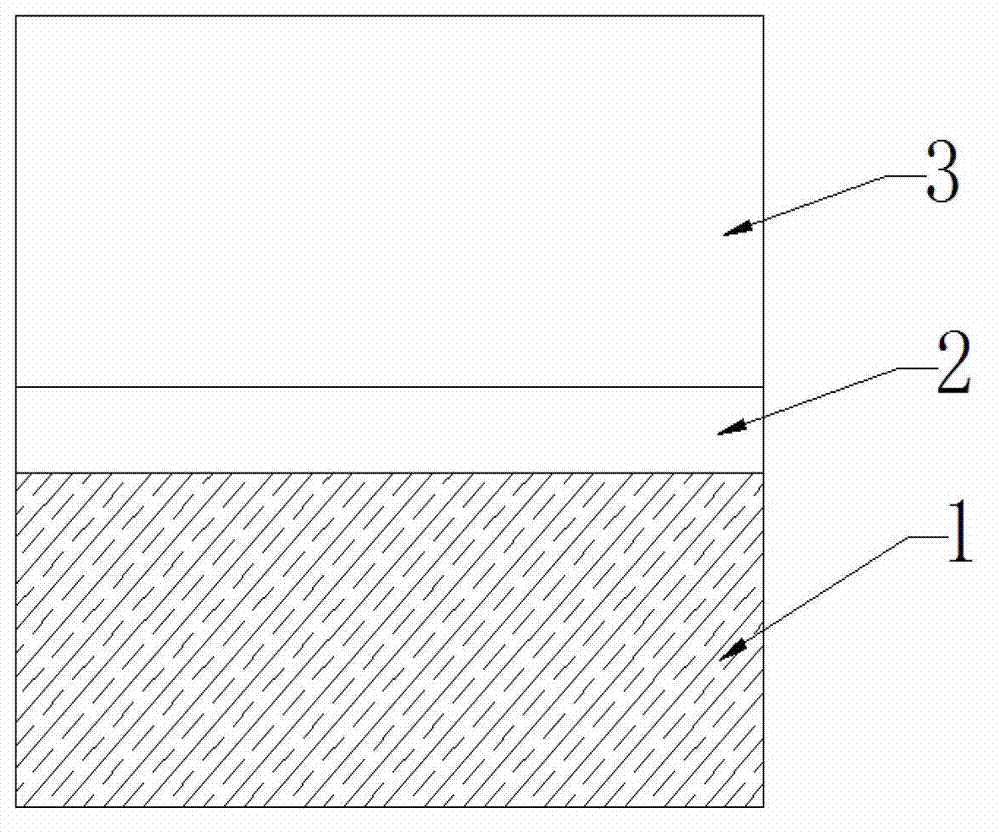
[0032] Step S04, performing a third wet etching on the device wafer to etch away the remaining device wafer body substrate 3;

[0033] In step S05, the device wafer is wet-etched to 5.4um for the fourth time.

[0034] The present invention adopts the process of multi-step grinding and etching. The more t...


PUM


Abstract

The invention relates to the field of semiconductors, in particular to a wafer back face thinning method. The wafer back face thinning method comprises the following steps: bonding a component wafer with a ground slide; conducting firs-time grinding on the back face of the component wafer; conducting first-time wet method etching on the component wafer; conducting second-time grinding on the back face of the component wafer; conducting second-time wet method etching on the component wafer; conducting third-time wet method etching on the component wafer; and conducting fourth-time wet method etching on the component wafer. Consequently, the component wafer is thinned to the required thickness. The wafer back face thinning method has the advantages of repeating grinding the back face of the component wafer and wet method etching in the original technological process, effectively reducing inner stress produced in the process of thinning the wafer after optimizing the technology through multi-step grinding and wet method etching, reducing fragment possibilities, and increasing the rate of finished products.

Description

technical field [0001] The invention relates to the field of semiconductors, in particular to a wafer back thinning method. Background technique [0002] The backside of the device wafer needs to be thinned in the manufacture of the back-illuminated image sensor, and the existing method for thinning the device wafer is generally grinding and wet etching. Grinding thinning speed is fast, which has a good effect on productivity improvement, but grinding can easily cause wafer cracks, increase internal stress, and the difference in surface thickness is obvious, so it is easy to cause wafer fragments in the subsequent process. Wet etching can relieve the internal stress caused by grinding and make the surface have better thickness uniformity, but the thinning rate is slow. At present, the commonly used process for thinning device wafers is to perform one grinding after bonding the device wafer to the carrier, and then perform multiple wet etching. Although this process method u...

Claims


Application Information

Patent Timeline
Patent Type & Authority Applications(China)
IPC IPC(8): H01L21/306
Inventor 李平
Owner WUHAN XINXIN SEMICON MFG CO LTD
Why Eureka
Try Eureka