Silicon-avalanche photodetector (Si-APD) with black silicon as photosensitive layer and preparation method thereof

A photodetector and photosensitive layer technology, applied in the field of photodetection, can solve the problems of expensive InGaAs crystal material, limited spectral detection range, poor thermal and mechanical properties, etc., to reduce lateral dark current, improve responsivity and quantum efficiency, The effect of improving the light absorption rate

Inactive Publication Date: 2013-06-05
UNIV OF ELECTRONICS SCI & TECH OF CHINA
View PDF5 Cites 17 Cited by
  • Summary
  • Abstract
  • Description
  • Claims
  • Application Information

AI Technical Summary

Problems solved by technology

[0006] Aiming at the above-mentioned prior art, the technical problem to be solved by the present invention is: the InGaAs crystal material has the disadvantages of high price, poor thermomechanical performance, poor crystal quality and difficulty in being compatible with the existing silicon microelectronics process; The band width is large, and the traditional Si-APD photodetector has the disadvantages of low responsivity and limited spectral detection range

Method used


Image

  • Silicon-avalanche photodetector (Si-APD) with black silicon as photosensitive layer and preparation method thereof
  • Silicon-avalanche photodetector (Si-APD) with black silicon as photosensitive layer and preparation method thereof
  • Silicon-avalanche photodetector (Si-APD) with black silicon as photosensitive layer and preparation method thereof

Examples


Embodiment Construction

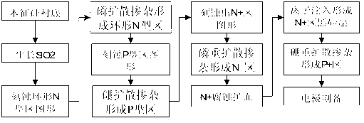
[0035] The specific implementation method of the present invention will be further described below in conjunction with the drawings and embodiments.

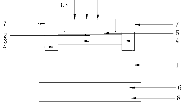
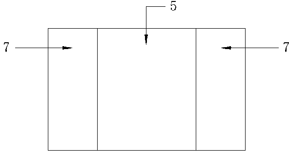
[0036] A Si-APD photodetector with black silicon as the photosensitive layer, such as figure 1 , 2 As shown, it includes silicon intrinsic substrate 1, N located in the center of the upper surface of silicon intrinsic substrate 1 + District 2, located in N + The P-type region 3 below the region 2, the ring-shaped N-type region 4 located around the upper surface of the silicon intrinsic substrate 1, and the N-type region located at the N + N on the upper surface of zone 2 + Region black silicon layer 5, P located on the lower surface of silicon intrinsic substrate 1 + District 6, located in N + The upper electrode 7 on the upper surface of the black silicon layer 5 and the ring-shaped N-type region 4 and the P + The lower electrode 8 on the lower surface of the region 6.

[0037] Among the above technical solutions:

[00...


PUM


Abstract

The invention discloses a silicon-avalanche photodetector (Si-APD) with black silicon as a photosensitive layer and a preparation method of the Si-APD with the black silicon as the photosensitive layer, and belongs to the field of photoelectric detection technology. The Si-APD comprises a silicon intrinsic substrate 1, an N<+> region 2, a P type region 3, an annular N type region 4, an N<+> region black silicon layer 5, a P<+> region 6, an upper electrode 7 and a lower electrode 8, wherein the N<+> region 2 is located in the middle of the upper surface of the silicon intrinsic substrate 1, the P type region 3 is located below the N<+> region, the annular N type region 4 is located on the periphery of the upper surface of the silicon intrinsic substrate, the N<+> region black silicon layer 5 is located on the upper surface of the N<+> region, the P<+> region 6 is located on the lower surface of the silicon intrinsic substrate, the upper electrode 7 is located on the upper surfaces of the N<+> region black silicon layer and the annular N type region, and the lower electrode 8 is located on the lower surface of the P<+> region. According to the Si-PAD, the black silicon material serves as the photosensitive layer, and meanwhile the annular N type region is additionally arranged on the peripheries of the N<+> region and the P type region. Thus, the Si-APD with the black silicon as the photosensitive layer can absorb light waves of a near-infrared band and have higher light absorptivity and a wider response wave band, the preparation technique is simple, the cost is low, and the Si-PAD has the advantages of being easy to integrate, quick in response speed, high in responsivity and wide in response wave band.

Description

technical field [0001] The invention belongs to the technical field of photoelectric detection, and relates to the structure of a photoelectric detection device, in particular to a Si-APD photodetector with a black silicon material as a photosensitive layer and a preparation method thereof. Background technique [0002] As an important part of optical fiber communication system, infrared imaging system, laser warning system and laser ranging system, photoelectric detectors have been widely used in civilian and military applications. APD is a photodetector with internal gain capability and high sensitivity, which is widely used in ultra-high-speed optical communication, signal processing, measurement and sensing systems. APD is a photodetector widely used in modern high-bit-rate optical communication systems. It has been widely used in weak light field measurement, photon Counting and other related fields. Because the APD photodetector has the characteristics of higher inte...

Claims


Application Information

Patent Timeline
Patent Type & Authority Applications(China)
IPC IPC(8): H01L31/107H01L31/0352H01L31/028H01L31/18
CPCY02P70/521Y02P70/50
Inventor 李伟王垠郭安然余峰王涛蒋亚东
Owner UNIV OF ELECTRONICS SCI & TECH OF CHINA
Why Eureka
Try Eureka