Method and structure of light emitting diode (LED) packaging
A technology of LED packaging and LED chips, applied in electrical components, circuits, semiconductor devices, etc., can solve the problems of low air tightness, affecting service life, aging of silica gel, etc., and achieve good air tightness, strong adhesion, The effect of improving stability and reliability
- Summary
- Abstract
- Description
- Claims
- Application Information
AI Technical Summary
Problems solved by technology
Method used
Image

Examples
Embodiment Construction
[0019] In order to make the object, technical solution and advantages of the present invention clearer, the present invention will be further described in detail below in conjunction with the accompanying drawings and embodiments. It should be understood that the specific embodiments described here are only used to explain the present invention, not to limit the present invention.
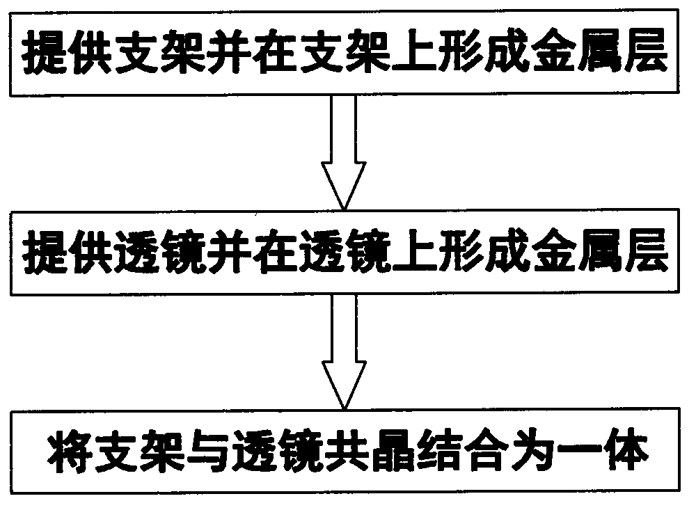
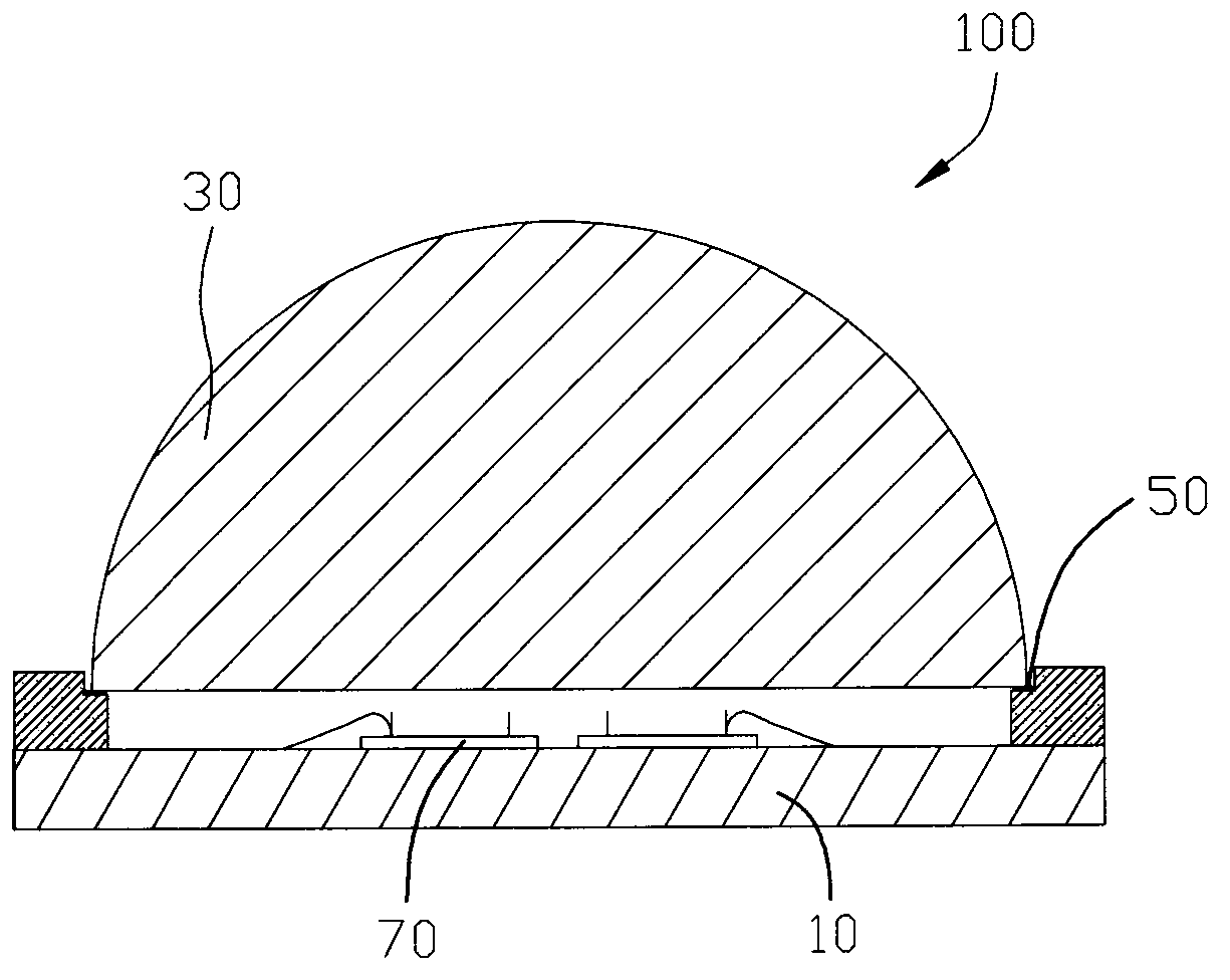
[0020] see figure 1 and figure 2 , figure 1 It is a flow chart of the LED encapsulation method of the present invention, figure 2 for figure 1 A schematic diagram of the LED structure 100 obtained by the method shown. Such as figure 1 As shown, the LED packaging method of the present invention mainly includes the following steps:
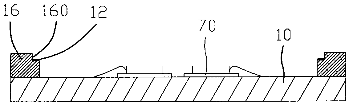
[0021] providing a bracket 10 and forming a metal layer 12 on the bracket 10;
[0022] providing a lens 30 and forming a metal layer 32 on the lens 30;
[0023] Install the lens 30 on the support 10 and carry out the die-bonding combination of the support 10 an...
PUM
 Abstract
Description
Claims
Application Information
 - R&D
- Intellectual Property
- Life Sciences
- Materials
- Tech Scout
- Unparalleled Data Quality
- Higher Quality Content
- 60% Fewer Hallucinations
Browse by: Latest US Patents, China's latest patents, Technical Efficacy Thesaurus, Application Domain, Technology Topic, Popular Technical Reports.
© 2025 PatSnap. All rights reserved.Legal|Privacy policy|Modern Slavery Act Transparency Statement|Sitemap|About US| Contact US: help@patsnap.com