Top-emitting organic electroluminescence device and manufacturing method thereof

A luminescence and top emission technology, which is applied in the fields of electrical solid-state devices, semiconductor/solid-state device manufacturing, electrical components, etc., can solve the problems of difficulty in obtaining lumen efficiency and low light output rate, and achieve the goal of improving lumen efficiency and increasing output rate Effect

Inactive Publication Date: 2013-06-05
OCEANS KING LIGHTING SCI&TECH CO LTD +1
View PDF4 Cites 4 Cited by
  • Summary
  • Abstract
  • Description
  • Claims
  • Application Information

AI Technical Summary

Problems solved by technology

[0007] The purpose of the present invention is to overcome the low light emission rate in the existing top-emitting organic electroluminescent device, and it is difficult to obtain satisfactory lumen efficiency, and to provide a light emission rate that can greatly improve the lumen efficiency. Top-emitting organic electroluminescent device and method of manufacturing the same

Method used


Image

  • Top-emitting organic electroluminescence device and manufacturing method thereof
  • Top-emitting organic electroluminescence device and manufacturing method thereof

Examples


Embodiment 1

[0042] Example 1: A top-emitting organic electroluminescent device was prepared according to the following steps.

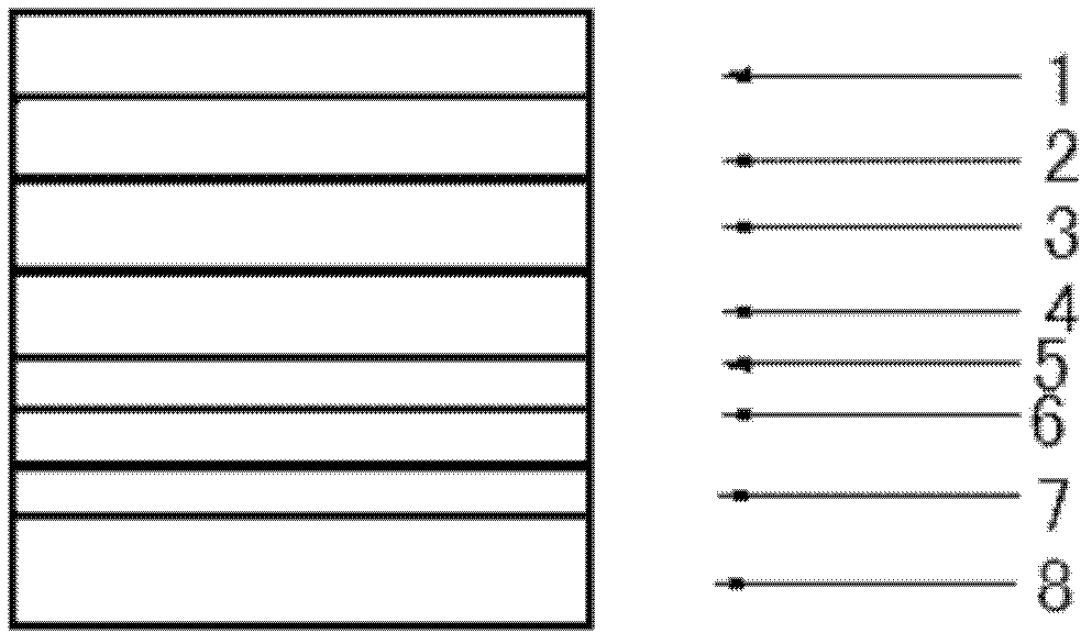
[0043] Sonicate the glass substrate sequentially with detergent, deionized water, acetone, ethanol, and isopropanol for 15 minutes each to remove organic pollutants on the glass surface. Next, the anode is vacuum-evaporated sequentially, the material is Ag, and the thickness is 120nm; the hole injection layer, the material is MoO 3 , the thickness is 30nm; the hole transport layer, the material is TAPC, the thickness is 30nm; the light emitting layer, the material is Alq 3 , thickness is 20nm; electron transport layer, material is TPBI, thickness is 50nm; electron injection layer, material is CsN 3 , with a thickness of 3 nm; and a cathode, made of Ag, with a thickness of 20 nm.

[0044] Next, using isopropanol as a solvent, 35% by weight of P25 titanium dioxide particles and 20% by weight of Triton X-100 emulsifier were added, stirred for 24 hours, and a titan...

Embodiment 2

[0047] Example 2: A top-emitting organic electroluminescent device was prepared according to the following steps.

[0048] Sonicate the glass substrate sequentially with detergent, deionized water, acetone, ethanol, and isopropanol for 15 minutes each to remove organic pollutants on the glass surface. Next, the anode is vacuum-evaporated sequentially, the material is Al, and the thickness is 250nm; the hole injection layer, the material is WO 3 , with a thickness of 20nm; the hole transport layer, made of NPB, with a thickness of 60nm; the light-emitting layer, made of DCJTB, with a thickness of 50nm; the electron transport layer, made of TAZ, with a thickness of 40nm; the electron injection layer, made of LiF, with a thickness of is 0.7nm; and the cathode is made of Ag and has a thickness of 30nm.

[0049] Next, using isopropanol as a solvent, 25% by weight of P25 titanium dioxide particles and 15% by weight of Triton X-100 emulsifier were added, stirred for 24 hours, and a ...

Embodiment 3

[0052] Example 3: A top-emitting organic electroluminescent device was prepared according to the following steps.

[0053] Sonicate the glass substrate sequentially with detergent, deionized water, acetone, ethanol, and isopropanol for 15 minutes each to remove organic pollutants on the glass surface. Next, the anode is vacuum-evaporated sequentially, the material is Au, and the thickness is 80nm; the hole injection layer, the material is V 2 o 5 , the thickness is 25nm; the hole transport layer, the material is TCTA, the thickness is 20nm; the light emitting layer, the material is TCTA: Firpic, the doping ratio is 20%, the thickness is 25nm; the electron transport layer, the material is TAZ, the thickness is 50nm; The electron injection layer is made of LiF with a thickness of 0.5nm; and the cathode is made of Ag with a thickness of 50nm.

[0054] Next, using isopropanol as a solvent, 40% by weight of P25 titanium dioxide particles and 15% by weight of Triton X-100 emulsifi...


PUM


Abstract

The invention discloses a top-emitting organic electroluminescence device and a manufacturing method thereof. The top-emitting organic electroluminescence device comprises a substrate, a positive electrode, a hole injection layer, a hole transmission layer, a luminescent layer, an electron transmission layer, an electron injection layer and a negative electrode, wherein a titanium dioxide antireflection film is formed on the negative electrode. The manufacturing method of the top-emitting organic electroluminescence device comprises a procedure that the titanium dioxide antireflection film is formed on the negative electrode. Compared with a top-emitting organic electroluminescence device in the prior art, the top-emitting organic electroluminescence device has the advantages that the light emitting rate is high, and luminous efficiency is greatly improved.

Description

technical field [0001] The invention relates to a top emission organic electroluminescent device and a preparation method thereof. Background technique [0002] In 1987, C.W.Tang and Van Slyke of Eastman Kodak Company in the United States reported a breakthrough in organic electroluminescence research, using ultra-thin film technology to prepare a high-brightness, high-efficiency double-layer organic electroluminescent device (OLED). In this double-layer structure device, the brightness reaches 1000 cd / m at 10V 2 , its luminous efficiency is 1.51 lm / W, and its lifespan is more than 100 hours. [0003] The principle of OLED light emission is based on the action of an external electric field, electrons are injected from the cathode to the lowest unoccupied molecular orbital (LUMO) of organic matter, and holes are injected from the anode to the highest occupied orbital (HOMO) of organic matter. Electrons and holes meet and recombine in the light-emitting layer to form exciton...

Claims


Application Information

Patent Timeline
Patent Type & Authority Applications(China)
IPC IPC(8): H01L51/52H01L51/56
Inventor 周明杰王平黄辉梁禄生
Owner OCEANS KING LIGHTING SCI&TECH CO LTD
Why Eureka
Try Eureka