Optical proximity correction method
A technology of optical proximity correction and lithography process, which is applied in the field of lithography process, and can solve the problems of increasing the difficulty of masking in mask factories and large errors in irregular parts.
- Summary
- Abstract
- Description
- Claims
- Application Information
AI Technical Summary
Problems solved by technology
Method used
Image


Examples
Embodiment Construction
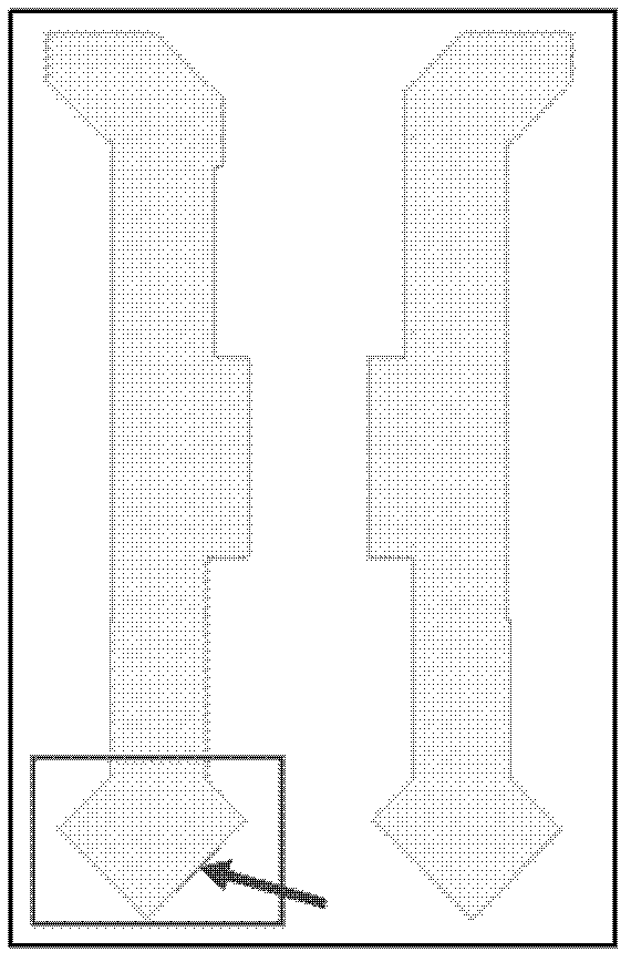
[0031] The CD (critical dimension) of the key layers of the technology node below 0.13um, such as TO (active area level), GT (gate oxide level), and An (metal wiring level), is getting smaller and smaller, and CD is close to or even smaller than lithography The wavelength of the light wave used in the process, so in the photolithography process, due to the diffraction and interference of light, there is a certain deformation and deviation between the photolithography pattern obtained on the actual silicon wafer and the mask pattern. This kind of error directly affects circuit performance and production yield. In order to eliminate this kind of error as much as possible, an effective method is the optical proximity correction (OPC) method. As mentioned in the background technology, at present, due to the needs provided by customers, OPC correction processing graphics are becoming more and more complex, and due to the needs of different customers, many parts that do not conform t...
PUM
 Abstract
Description
Claims
Application Information
 - R&D
- Intellectual Property
- Life Sciences
- Materials
- Tech Scout
- Unparalleled Data Quality
- Higher Quality Content
- 60% Fewer Hallucinations
Browse by: Latest US Patents, China's latest patents, Technical Efficacy Thesaurus, Application Domain, Technology Topic, Popular Technical Reports.
© 2025 PatSnap. All rights reserved.Legal|Privacy policy|Modern Slavery Act Transparency Statement|Sitemap|About US| Contact US: help@patsnap.com