Method for preparing non-polar GaN film on r-face sapphire substrate

A sapphire substrate, non-polar technology, used in semiconductor/solid-state device manufacturing, electrical components, circuits, etc., can solve problems such as poor quality of non-polar GaN crystals, improve international competitiveness, reduce production costs, and solve The effects of the energy crisis

Inactive Publication Date: 2013-06-12
BEIJING UNIV OF TECH
View PDF6 Cites 3 Cited by
  • Summary
  • Abstract
  • Description
  • Claims
  • Application Information

AI Technical Summary

Problems solved by technology

[0004] In order to solve the problem of poor quality of a-plane non-polar GaN crystals, the object of the present invention is to provide a method for heteroepitaxial non-polar a-plane (11-20) GaN thin film materials on r-plane sapphire by MOCVD technology, including the following steps :

Method used


Image

  • Method for preparing non-polar GaN film on r-face sapphire substrate
  • Method for preparing non-polar GaN film on r-face sapphire substrate
  • Method for preparing non-polar GaN film on r-face sapphire substrate

Examples


Embodiment Construction

[0025] The present invention will be described in further detail below in combination with specific embodiments and accompanying drawings.

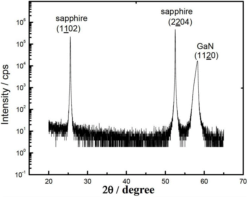
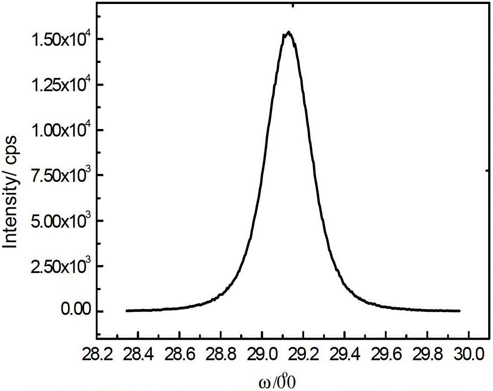
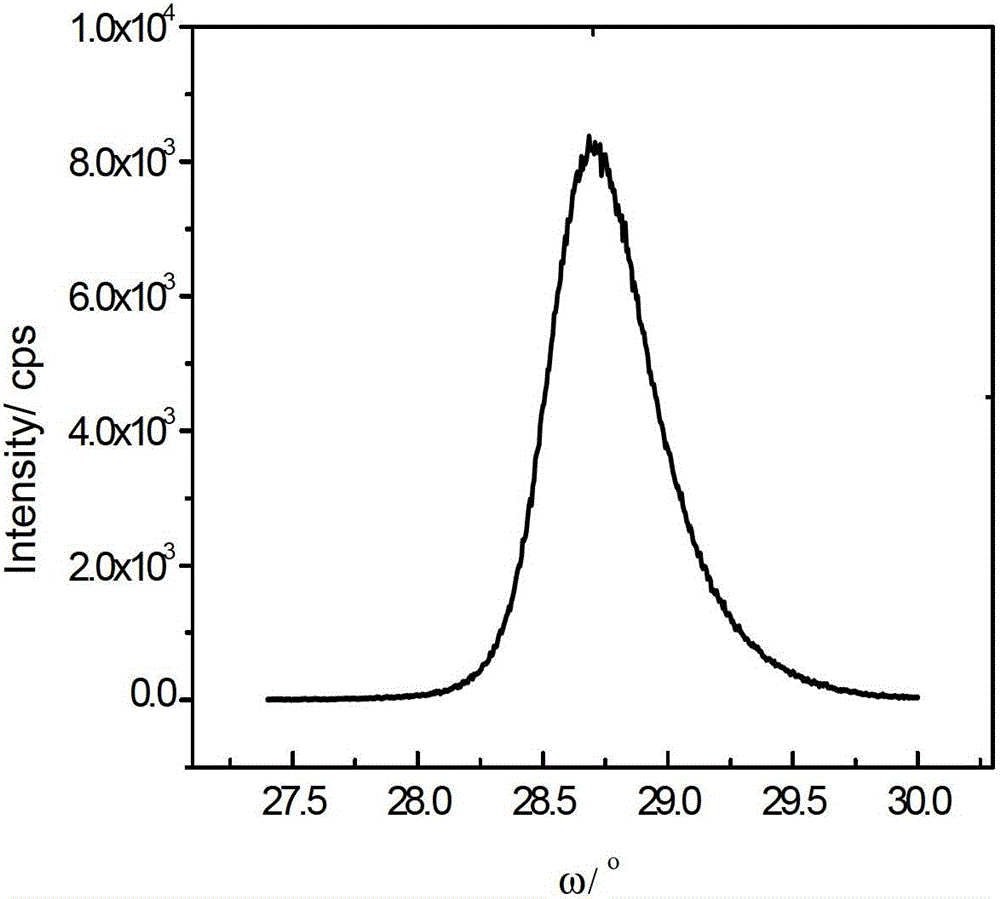
[0026] This embodiment is a method for preparing a non-polar GaN film grown on an r-plane sapphire substrate, including the following steps:

[0027] (1) Select the substrate: use the r-plane sapphire substrate, and the orientation of the substrate is 45° off the a-axis

[0028] (2) Using metal-organic chemical vapor deposition (MOCVD) technology, epitaxial non-polar GaN film buffer layer in D125 equipment, the process conditions are: firstly, the substrate is cleaned at high temperature: the substrate is baked at 1100 °C After about 4 hours, reduce the temperature of the reaction chamber, the substrate temperature is 525°C, the reaction chamber pressure is 500torr, V / III is 1700, the thickness of the buffer layer is 25nm, and the carrier gas is hydrogen.

[0029] (3) High-temperature growth a-plane (11-20) GaN process conditions: increa...


PUM


Abstract

The invention discloses a method for preparing a non-polar GaN film on an r-face sapphire substrate and belongs to the field of LED (light-emitting diode) devices. Metal-organic chemical vapor deposition (MOCVD) equipment is adopted to prepare a non-polar (11-22)-face GaN film on the r-face sapphire substrate. The high temperature growth non-polar GaN film V / III ratio adopts a three-step growth technology, namely the V / III ratio is from low to high, and then to low (low-high-low). The low V / III ratio is 180-220, the high V / III ratio is 2800-3200, and H2 is used as carrier gas for growth. The method has the characteristics that the growth design of each stage provides guarantee for the growth in the next stage, the former low V / III growth condition restrains different crystal orientation growth speed difference and provides a high-quality template for the GaN growth of the high V / III growth in the next stage, and the smoother non-polar (11-20)-face GaN film without empty hole defects is obtained under the low V / III growth condition.

Description

technical field [0001] The invention relates to a technology and method for growing non-polar GaN thin films on an r-plane sapphire substrate by metal organic chemical vapor deposition (MOCVD), and belongs to the field of semiconductor material preparation. Background technique [0002] The current commercially produced GaN-based LEDs epitaxially grow the hexagonal wurtzite structure on the c-plane sapphire substrate along the [1000] polar axis direction. GaN materials grown along the [1000] polar axis direction have strong spontaneous polarization and piezoelectric polarization, and the polarization electric field causes the quantum-confined Stark effect in the active region of the LED, which reduces the recombination efficiency of the light-emitting device and red-shifts the emission wavelength. , reducing the performance of optoelectronic devices. In order to solve the polarization problem, research on non-polar GaN materials was carried out, using different substrate ma...

Claims


Application Information

Patent Timeline
Patent Type & Authority Applications(China)
IPC IPC(8): H01L21/205H01L33/02
Inventor 邢艳辉韩军
Owner BEIJING UNIV OF TECH
Why Eureka
Try Eureka