An array substrate of a display panel and a manufacture method thereof

A technology for array substrates and display panels, applied in semiconductor/solid-state device manufacturing, electrical components, transistors, etc., can solve the problems of unfavorable display panel production and development, process control difficulty, and cost increase

Active Publication Date: 2013-06-12
AU OPTRONICS CORP
View PDF5 Cites 19 Cited by
  • Summary
  • Abstract
  • Description
  • Claims
  • Application Information

AI Technical Summary

Problems solved by technology

However, as the resolution increases, the number of thin film transistors (TFT) on the panel also increases, making the available space on the panel continuously shrinking
At the same time, in order to improve the aperture ratio and the performance of thin film transistors, the number of PEPs has been increased in the process design
However,

Method used


Image

  • An array substrate of a display panel and a manufacture method thereof
  • An array substrate of a display panel and a manufacture method thereof
  • An array substrate of a display panel and a manufacture method thereof

Examples


Embodiment Construction

[0027] In order to enable those who are familiar with the technical field of the present invention to further understand the present invention, preferred embodiments of the present invention are listed below, together with the accompanying drawings, to describe in detail the composition and effects of the present invention.

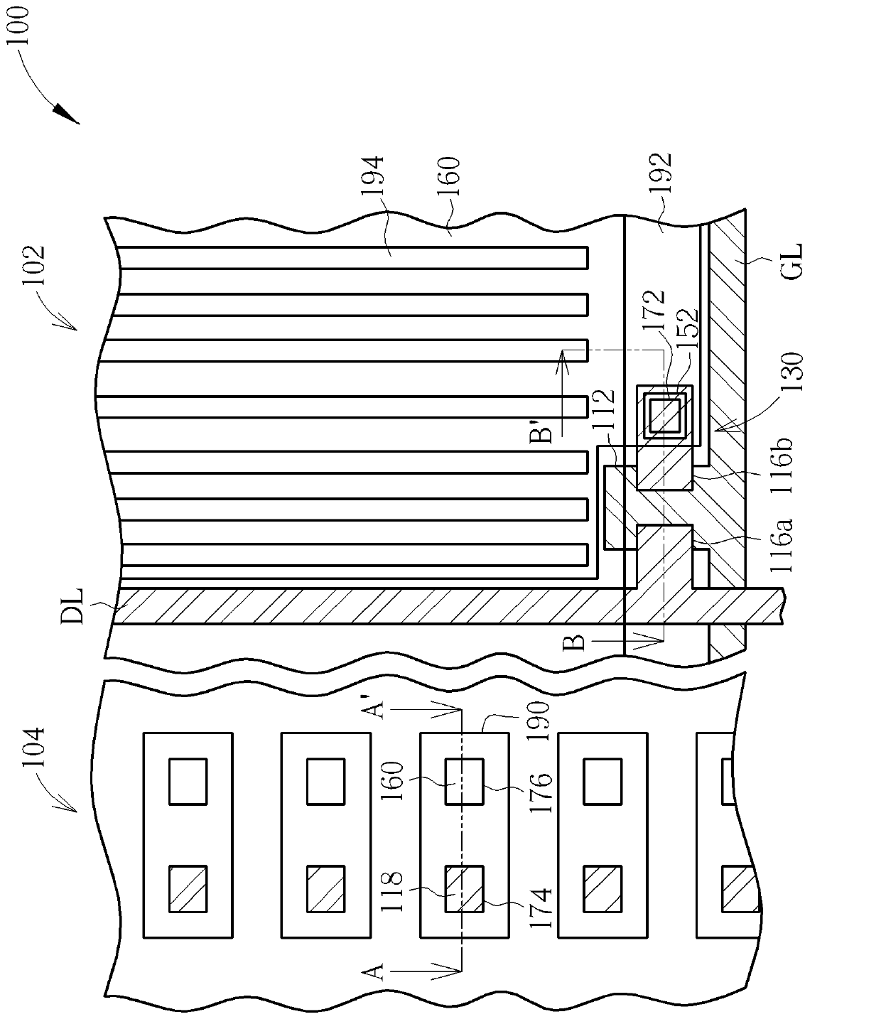
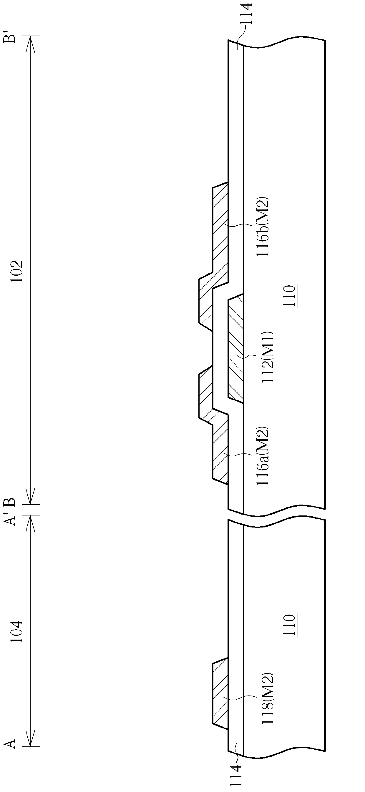
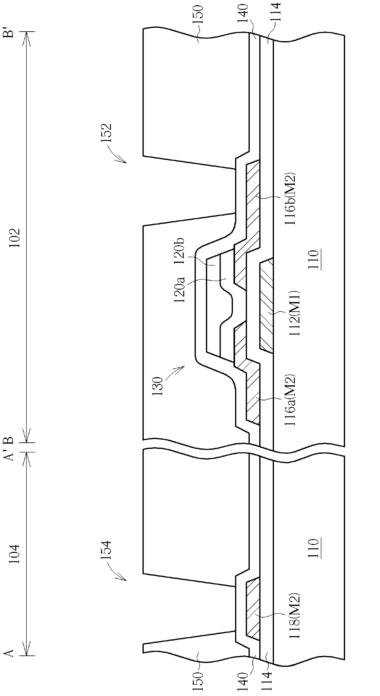
[0028] Please refer to Figure 1 to Figure 8 , Figure 1 to Figure 8 A schematic diagram showing a method for manufacturing an array substrate of a display panel provided by an embodiment of the present invention, wherein figure 1 is a schematic top view of the array substrate of the display panel provided in this embodiment, and Figure 2 to Figure 8 then shows figure 1 Schematic diagram of the cross-section obtained along the A-A' section line and the B-B' section line. Such as figure 1 and figure 2 As shown, a substrate 110 is provided first. The substrate 110 can be a rigid substrate such as a glass substrate, or a flexible substrate such as a...


PUM


Abstract

A method for manufacturing an array substrate of a display panel comprises the steps of providing a substrate, on which a thin film transistor and a connection electrode are formed; forming a first protection layer and a flat layer on the substrate, the flat layer comprising a first opening and second opening corresponding to the drain electrode of the thin film transistor and the connection electrode respectively; forming a common electrode, a second protection layer and a light resistance pattern layer which exposes the second protection layer disposed in the first opening and the second opening and corresponding to the common electrode; etching the second protection layer exposed by the light resistance pattern layer for forming a third opening, a fourth opening and a fifth opening; etching the first protection layer exposed by the third opening and the fourth opening for forming a sixth opening and a seventh opening and exposing the drain electrode and the connection electrode; and removing the light resistance pattern layer and forming a bridging electrode and a pixel electrode on the second protection layer.

Description

technical field [0001] The present invention relates to an array substrate of a display panel and a manufacturing method thereof, in particular to an array substrate of a display panel capable of reducing a photolithography and etching process (hereinafter referred to as PEP). Background technique [0002] Flat panel displays, such as liquid crystal displays, have replaced traditional cathode ray tube (CRT) displays and become the mainstream of displays due to their thinness, lightness, low radiation, and low power consumption. In the development of the display, it is constantly developing towards the direction of high resolution requirements. However, as the resolution increases, the number of thin film transistors (thin film transistor, TFT) on the panel also increases, so that the available space on the panel continues to shrink. At the same time, in order to improve the aperture ratio and the performance of the thin film transistor, the number of PEP is increased in the...

Claims


Application Information

Patent Timeline
IPC IPC(8): H01L21/77H01L27/02H01L29/786
Inventor 黄郁涵黄德群黄国有
Owner AU OPTRONICS CORP
Why Eureka
Try Eureka