Pec biasing technique for LEDs

A light-emitting diode, bias voltage technology, applied in circuits, electrical components, electrical solid devices, etc., can solve the problem that the N layer cannot be interconnected with metal interconnects.

Active Publication Date: 2013-06-12
LUMILEDS HLDG BV
View PDF4 Cites 1 Cited by
  • Summary
  • Abstract
  • Description
  • Claims
  • Application Information

AI Technical Summary

Problems solved by technology

[0006] Applicants have discovered that one problem with using interconnect metal on the substrate for biasing is that the traces connected to the N metal are exposed on the sidewalls after sawing the substrate wafer for singulation
Also, when forming multiple micro-LEDs in a single die, the N layer cannot be interconnected with the sawable interconnect metal

Method used


Image

  • Pec biasing technique for LEDs
  • Pec biasing technique for LEDs
  • Pec biasing technique for LEDs

Examples


Embodiment Construction

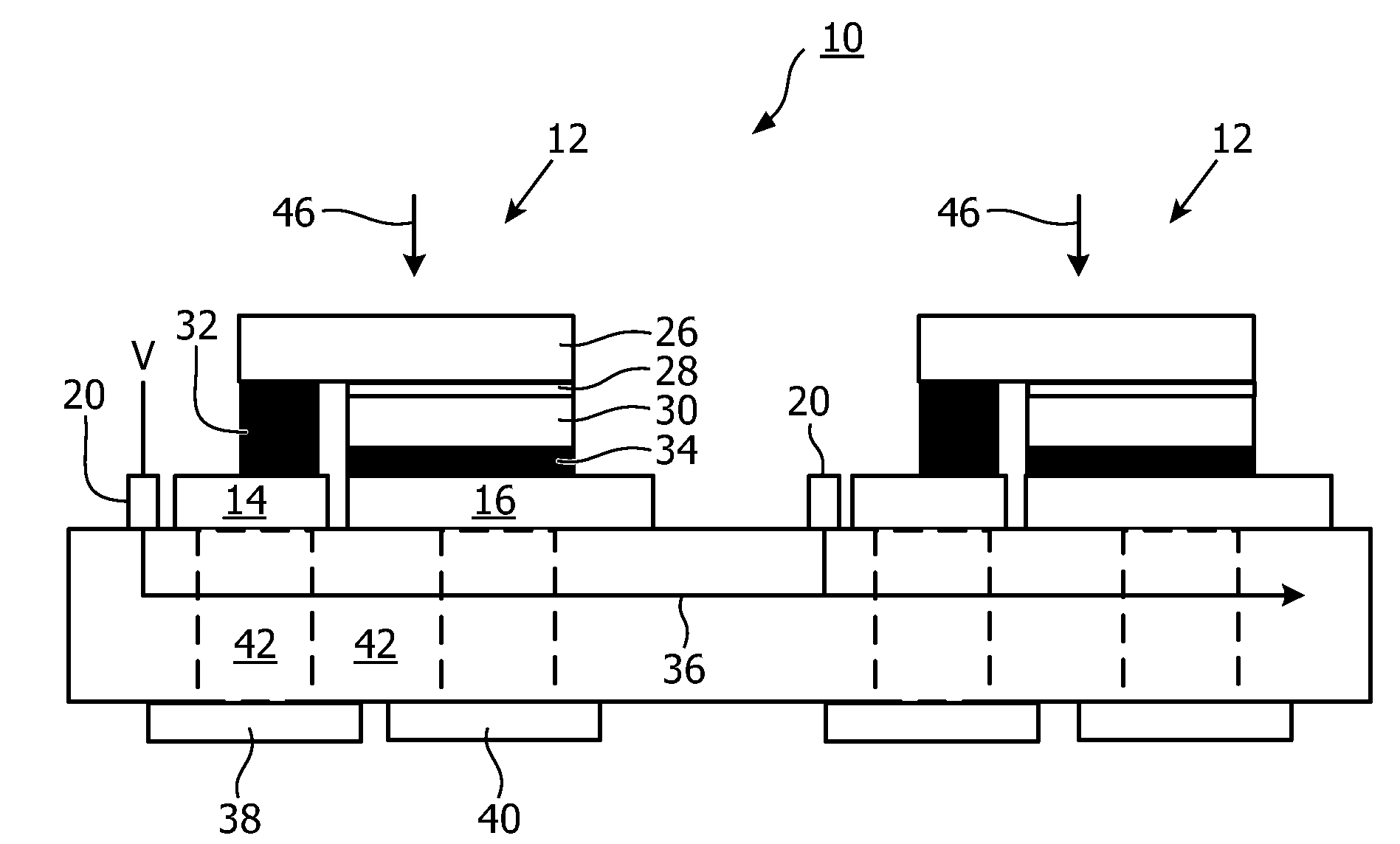
[0027] FIG. 1 shows a substrate wafer 10 populated with an array of LED dies 12 . There may be hundreds of dies 12 bonded to wafer 10 . The substrate base material can be ceramic, silicon, insulating aluminum or other materials.

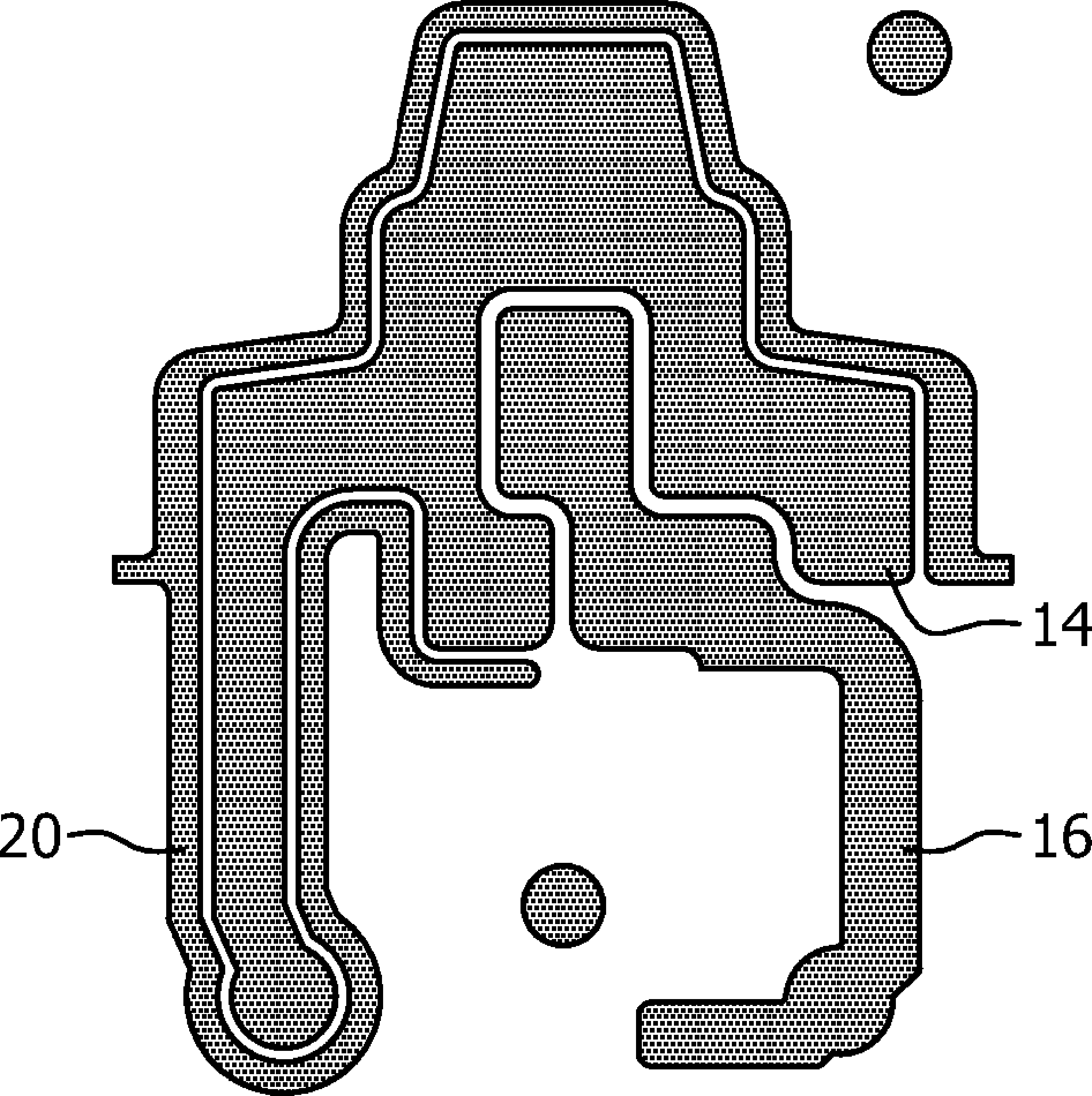
[0028] FIG. 2 is a close-up of four adjacent LED areas on wafer 10 showing N metal 14 and P metal 16 on the surface of wafer 10 . Metal 14 / 16 forms pads for bonding to the electrodes of LED die 12 . LED 12 and metal 14 / 16 can be any size. The metal 14 / 16 may be Ni / Au plated copper for bonding to the cathode and anode Ni / Au electrodes on the bottom surface of the LED die 12 . The LED electrodes can be bonded to the metal 14 / 16 by ultrasonic welding or other methods.

[0029] Metal 14 / 16 may be connected to the bottom pad of each substrate in wafer 10 by vias extending through wafer 10 . After singulation, the bottom pad can then be surface mounted on a printed circuit board.

[0030] Metal pattern 20 is formed very close to N-metal 14 (suc...


PUM


Abstract

Each LED in an array of LEDs mounted on a submount wafer has at least a first semiconductor layer exposed and connected to a first electrode of each LED. The submount wafer has a first metal portion bonded to the first electrode of each LED for providing an energization current to each LED. The submount wafer also has a second metal portion running along and proximate to the first metal portion but not electrically connected to the first metal portion. The second metal portion may be interdigitated with the first metal portion. The second metal portion is connected to a bias voltage. When the wafer is immersed in an electrically conductive solution for electrochemical (EC) etching of the exposed first semiconductor layer, the solution electrically connects the second metal portion to the first metal portion for biasing the first semiconductor layer during the EC etching.

Description

technical field [0001] The present invention relates to forming light emitting diodes (LEDs), and in particular, to a method for electrically biasing exposed LED layers during electrochemical etching. Background technique [0002] A typical flip-chip LED has reflective p- and n-contacts on the bottom surface of the LED, and these contacts connect directly to bond pads on the substrate. Light generated by the LED is primarily emitted through the top surface of the LED surface. In this way, there is no top contact blocking light, and no wire bonds are required. [0003] During fabrication, a substrate wafer is filled with an array of LED dies, and the LED dies are further processed on the wafer as a batch. Finally, the wafer is singulated by, for example, sawing. [0004] The efficiency of flip-chip gallium nitride (GaN) LEDs can be increased by removing the transparent sapphire growth substrate after all LED layers have been epitaxially grown. After removing the substrate...

Claims


Application Information

Patent Timeline
Patent Type & Authority Applications(China)
IPC IPC(8): H01L33/62H01L25/16H01L33/22
CPCH01L25/167H01L33/0095H01L33/22H01L33/62H01L2224/16H01L33/00H01L22/14H01L33/005
Inventor Y.魏
Owner LUMILEDS HLDG BV
Why Eureka
Try Eureka