PN junction thin film transistor non-volatilisation photoelectric detector

A technology of thin-film transistors and photodetectors, which is applied in semiconductor devices, circuits, electrical components, etc., can solve the problems of source-drain punch-through, short-channel effect, and drain-induced barrier reduction, achieving reduced pixel size and high dynamic Range, Mitigation Effects of further narrowing

Active Publication Date: 2013-06-19
NANJING UNIV
View PDF4 Cites 10 Cited by
  • Summary
  • Abstract
  • Description
  • Claims
  • Application Information

AI Technical Summary

Problems solved by technology

However, as the process size continues to shrink, they will face many problems such as short channel effects, source-drain punchthrough, and drain-induced barrier reduction.

Method used


Image

  • PN junction thin film transistor non-volatilisation photoelectric detector
  • PN junction thin film transistor non-volatilisation photoelectric detector
  • PN junction thin film transistor non-volatilisation photoelectric detector

Examples


Embodiment Construction

[0019] The structure of the detector of the present invention and its specific detection method will be described below with reference to the accompanying drawings.

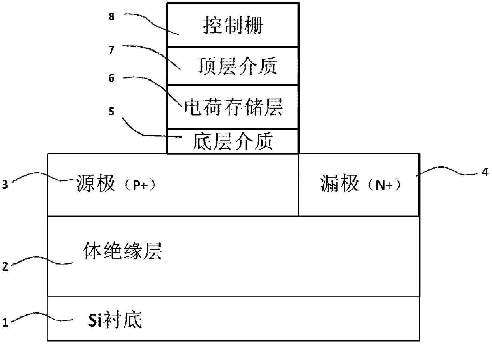
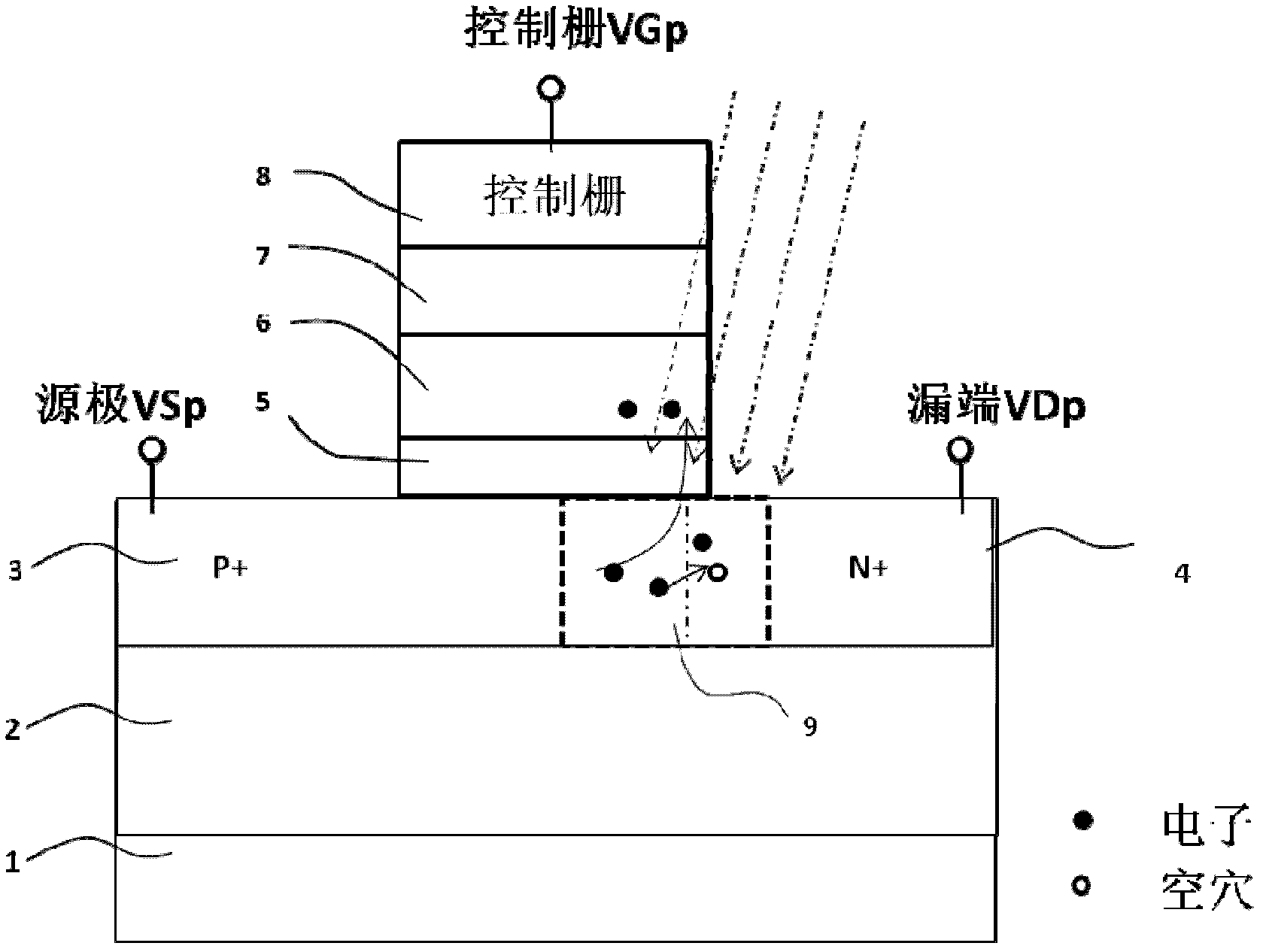
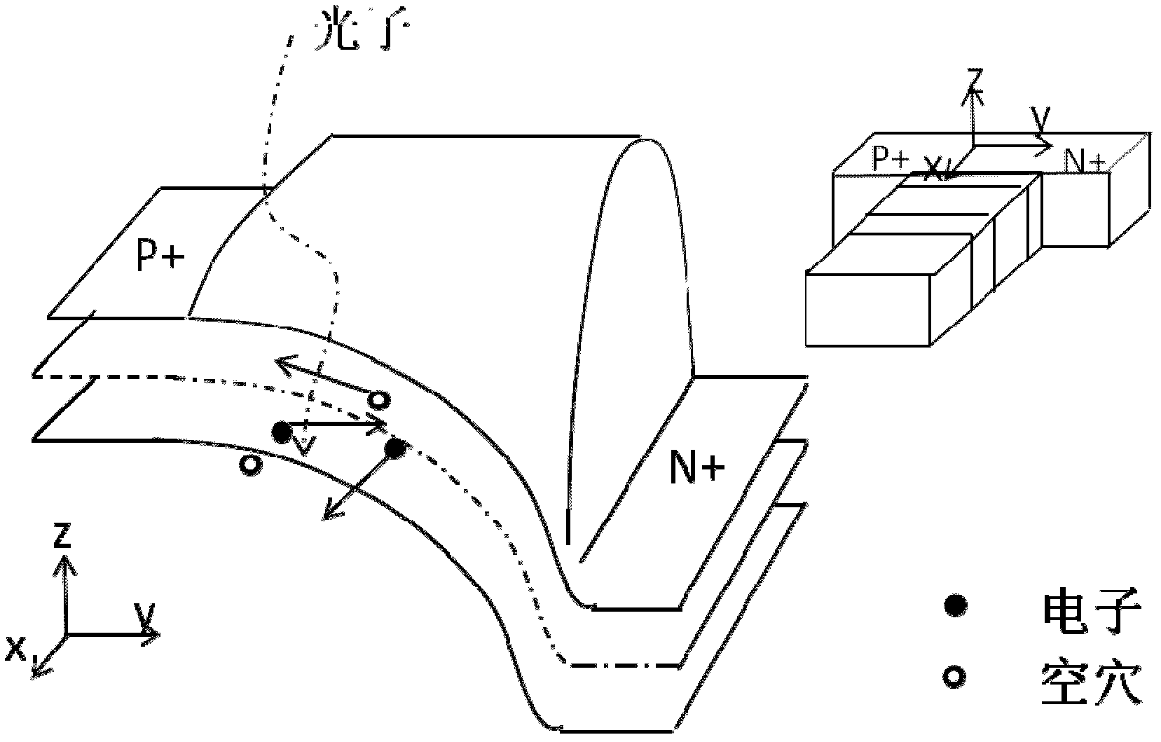
[0020] The basic structure of the detector of the present invention adopts a composite dielectric gate structure of a PN junction thin film transistor, such as figure 1 The basic structure of the detector of the present invention is shown, which is also similar to the composite dielectric grid photosensitive detector structure (refer to WO2010 / 094233, the thickness of the dielectric material can be referred to), the difference is that the structure of the present invention adopts a simpler three-terminal structure, including : Silicon (Si) substrate (1), a layer of insulating medium directly above the substrate is called a bulk insulating layer (2), and directly above the bulk insulating layer is a P-type source (3) that is doped with different semiconductor film layers and the N-type drain (4), at the source-dra...


PUM


Abstract

The invention discloses a PN junction thin film transistor non-volatilisation photoelectric detector. The detector structurally comprises a silicon (Si) substrate (1), wherein a layer of insulating media, namely a body insulating layer (2) is arranged over the substrate, a P-type source electrode (3) and an N-type drain electrode (4) which are formed by a semiconductor film layer with different dopings are arranged over the body insulating layer, and bottom layer insulating media (5), a charge storage layer (6), top layer insulating media (7) and a control grid electrode (8) are sequentially arranged from bottom to top over one side of the source electrode at the boundary of the source electrode and the drain electrode. The two layers of insulating media surround the charge storage layer to prevent middle charges from draining. The bottom layer insulating media enable a semiconductor layer and the charge storage layer to be isolated. At least one of the control grid electrode and the substrate is made of transmitting materials so as to achieve optical detection. By means of the PN junction thin film transistor non-volatilisation photoelectric detector, PN junction reversal of biasing is used for generating and collecting optical signals, and by measuring band to band tunneling (BTBT) currents of a PN junction, the signals can be read.

Description

technical field [0001] The invention relates to an imaging detection device, in particular to a working mechanism of the imaging detection device based on a thin film transistor non-volatile memory structure, which is a PN junction thin film transistor non-volatile photoelectric detector. Background technique [0002] Image sensors are widely used in today's society, such as mobile phones, digital cameras, various video cameras, and national defense detection fields. The main imaging detectors currently developed are CCD and CMOS-APS. CCD appeared earlier and the technology is relatively mature. , its basic structure is a series of MOS capacitors connected in series, and the generation and change of the potential well on the surface of the semiconductor is controlled by the voltage pulse sequence on the capacitor, so as to realize the storage and transfer readout of the photogenerated charge signal. Each pixel of CMOS-APS uses diodes and multiple Composed of transistors, by ...

Claims


Application Information

Patent Timeline
Patent Type & Authority Applications(China)
IPC IPC(8): H01L31/113H01L31/0224H01L31/18
CPCY02P70/50
Inventor 闫锋夏好广卜晓峰徐跃吴福伟马浩文
Owner NANJING UNIV
Why Eureka
Try Eureka