Micro-medium cone and nanometal grating-compounded optical probe

A metal grating and optical probe technology, applied in the field of optics and optoelectronics, can solve the problems of less collected light energy and small entrance of nano-metal cones, and achieve the effect of high spatial resolution and high sensitivity

Inactive Publication Date: 2013-06-26
NANKAI UNIV
View PDF3 Cites 18 Cited by
  • Summary
  • Abstract
  • Description
  • Claims
  • Application Information

AI Technical Summary

Problems solved by technology

[0003] The purpose of the present invention is to solve the problem of small entrance of the nano-metal cone and less light energy to be collected, and provide a high spatial resolution and high-sensitivity optical probe composed of a micro-medium cone and a nano-metal grating

Method used


Image

  • Micro-medium cone and nanometal grating-compounded optical probe
  • Micro-medium cone and nanometal grating-compounded optical probe
  • Micro-medium cone and nanometal grating-compounded optical probe

Examples


Embodiment 1

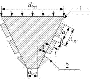
[0018] like figure 1 As shown, the optical probe with high spatial resolution and high sensitivity micro-dielectric cone and nano-metal grating compounded by the present invention is composed of micro-dielectric cone and nano-metal grating, and the refractive index of the micro-dielectric cone is n d , with a dielectric constant ε d , the large base of the micro-medium cone is the entrance of light energy, with a diameter of d inc , the small bottom surface of the micro-medium cone is the exit end of light energy, with a diameter of d out , d inc On the order of microns, d out At the nanoscale, the cone angle of the micromedia cone is 2θ. The nano-metal grating is distributed along the outer surface of the micro-medium cone, and the dielectric constant of the nano-metal grating is ε m , the period is Λ g , at the exit end of the light energy, the shape of the nanometal grating is tapered, the thickness changes linearly from t to 0, and the thickness of other parts is t. ...


PUM


Abstract

The invention provides a micro-medium cone and nanometal grating-compounded optical probe with high spatial resolution and high sensitivity. The optical probe consists of a micro-medium cone and nanometal gratings, wherein the nanometal gratings are distributed along the outer surface of the micro-medium cone, the micro-medium cone collects incident light energy with larger aperture as far as possible and gathers the light engery towards a cone top, the gathered light energy is efficiently coupled and converted into surface plasmons by the nanometal gratings, so that the surface plasmons can be continuously compressed and focused along with a cone surface, and a nano-focused high-local area strong field is formed at the tip end of the cone. In addition, regulation and optimization of nano focus can be realized through changing and optimizing the apex angle of the micro-medium cone, the structure and parameters of the gratings, and the size of an outlet. The optical probe can be used as a probe of a near field scanning microscope, an atomic force microscope and a tip-enhanced raman spectrometer, the strong nano focus formed by the optical probe can be used as a light source of nano lithography and sub-wavelength optical communication, and has important application values in the fields of nanosensing, nanoimaging, nano lithography, sub-wavelength optical communication and the like.

Description

technical field [0001] The invention belongs to the field of optics and photoelectric technology, and relates to micro-nano optical devices, surface plasmon excitation and nano-focusing, in particular to an optical probe with high spatial resolution and high sensitivity. Background technique [0002] How to efficiently gather, transmit and confine light energy in the nanometer region has become a key basic scientific and technical issue in the fields of photonics, plasmonics and nano-optics in recent years. Resolution and sensitivity are critical. The use of nano-metal structures to convert incident light into surface plasmons, and then guide them to highly confined nano-regions to form localized electromagnetic fields is the most effective and feasible way to break through the traditional optical diffraction limit to achieve hyperfocus. Various nanometal structure-guided surface plasmon modes have been proposed at home and abroad, mainly including nanometal particle chains...

Claims


Application Information

Patent Timeline
Patent Type & Authority Applications(China)
IPC IPC(8): G02B27/58
Inventor 匡登峰欧阳升
Owner NANKAI UNIV
Why Eureka
Try Eureka