Mixed substrate encapsulation method and mixed substrate encapsulation structure for semiconductor device

A technology of hybrid substrate and packaging method, which is applied in the direction of semiconductor devices, semiconductor/solid-state device manufacturing, semiconductor/solid-state device components, etc., can solve the problems of low mechanical strength of packaging structure, dust pollution, easy breakage, etc., and achieve a firm packaging structure Reliable, simplified packaging process, improved mechanical strength

Active Publication Date: 2013-06-26
GALAXYCORE SHANGHAI
View PDF8 Cites 10 Cited by
  • Summary
  • Abstract
  • Description
  • Claims
  • Application Information

AI Technical Summary

Problems solved by technology

[0005] 1) The above-mentioned encapsulation technology uses a whole piece of optical glass 105, and only the optical glass 105 provides strength. However, due to the overall brittleness of the glass, the mechanical strength of the encapsulation structure is low and it is easy to break; Expensive, thus increasing packaging costs;
[0006] 2) Since the cavity wall 103 is obtained by exposure and development of photosensitive materials, its cost of raw materials and process costs are high, and th

Method used


Image

  • Mixed substrate encapsulation method and mixed substrate encapsulation structure for semiconductor device
  • Mixed substrate encapsulation method and mixed substrate encapsulation structure for semiconductor device
  • Mixed substrate encapsulation method and mixed substrate encapsulation structure for semiconductor device

Examples


Embodiment 1

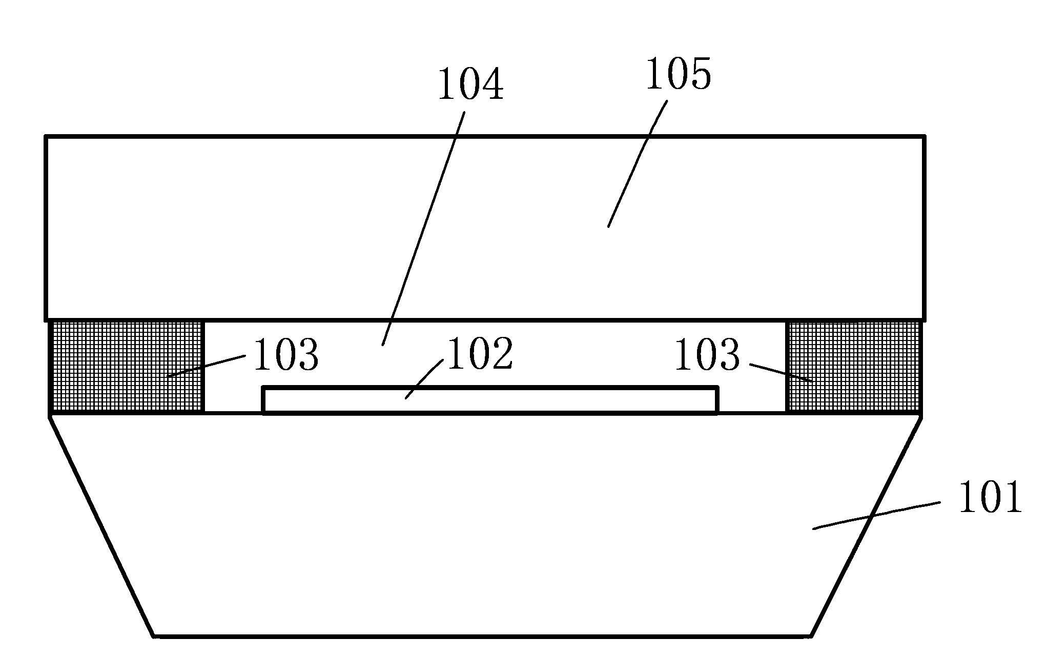
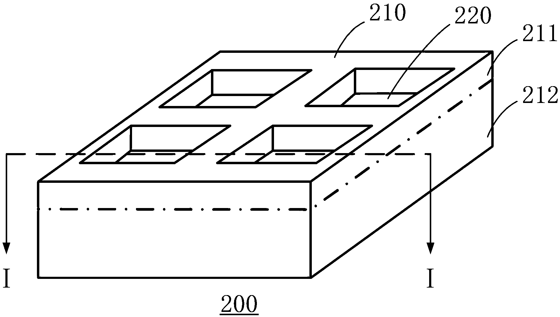
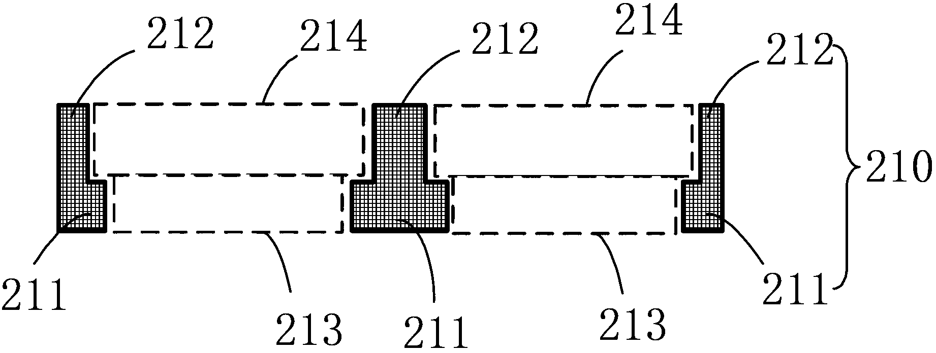
[0058] Please refer to figure 2 , the present embodiment provides a hybrid substrate 200 including a support frame 210 and a transparent substrate 220 . The supporting frame 210 includes a frame bottom 211 and a frame wall 212 . exist figure 2 In , the hybrid substrate 200 is placed upside down, so the part above the dot-dash line in the support frame 210 is the frame bottom 211 , and the part below the dot-dash line is the frame wall 212 . The frame bottom 211 includes a first through hole for exposing the pixel unit of the image sensor ( figure 2 Not marked in, please refer to Figure 3a dashed box in 213).

[0059] In this embodiment, the frame bottom 211 and the frame wall 212 of the supporting frame 210 are made of the same material, and the material for making it may preferably be ceramic material, flame-resistant resin material, glass material or silicon material. Further preferably, the frame bottom 211 and the frame wall 212 of the support frame 210 may be int...

Embodiment 2

[0069] Please refer to Figure 5 , Figure 5 It is a schematic cross-sectional view of a hybrid substrate 500 according to Embodiment 2 of the present invention. Most of the structure of the hybrid substrate 500 provided in the present embodiment is the same as that of the hybrid substrate 200 provided in the first embodiment. For the same part, refer to the content in Embodiment 1. The hybrid substrate 500 of this embodiment is different from the hybrid substrate 200 in the first embodiment in that, in the transparent substrate 520 of the hybrid substrate 500 , both the upper surface and the lower surface include an optical coating 510 . The optical coating 510 may be an IR (infrared) film or an AR (anti-reflect) film (anti-reflection film, also called anti-reflection film or anti-reflection film), or a laminate of the two. The IR film can allow visible light to pass through the lens and cut off or reflect infrared light, so that the packaged semiconductor device will not ...

Embodiment 3

[0073] Please continue to refer Figure 6 , Figure 6 It is a schematic cross-sectional view of a hybrid substrate 600 according to Embodiment 3 of the present invention. The hybrid substrate 600 provided in this embodiment has the same partial structure as the hybrid substrate 200 provided in the first embodiment. For the same part, refer to the content in Embodiment 1. The difference between the hybrid substrate 600 in this embodiment and the hybrid substrate 200 in Embodiment 1 is that the frame bottom 611 and the frame wall 612 are made of the same material, and then bonded together to form a support frame 610 .

[0074] Similar to the first embodiment, the frame bottom 611 and the frame wall 612 are preferably made of ceramic material, flame-resistant resin material, glass material or silicon material. Further preferably, the frame bottom 611 and the frame wall 612 can be integrally formed of ceramic material, flame-resistant resin material or silicon material, for exa...


PUM


Abstract

The invention provides a mixed substrate encapsulation method and a mixed substrate encapsulation structure for a semiconductor device. A mixed substrate is used for encapsulating the semiconductor device and comprises a support frame and a transparent substrate. The support frame comprises a frame bottom and a frame wall which are connected with each other, wherein the frame bottom is provided with a first through hole, the frame wall is provided with a second through hole, the area of the first through hole is smaller than that of the second through hole, and the first through hole is communicated with the second through hole. The transparent substrate is located in the second through hole and fixed on the upper surface of the frame bottom or the side of the frame wall. A first micropore is arranged between the transparent substrate and the frame bottom. A second micropore is arranged between the transparent substrate and the frame wall. The first micropore is communicated with the second micropore. The strength of the mixed substrate is much higher than that of a large optical glass, so that yield and efficiency of the mixed substrate encapsulation structure and the mixed substrate encapsulation method are increased while cost is reduced.

Description

technical field [0001] The invention relates to the field of semiconductor packaging, in particular to a hybrid substrate, a semiconductor device packaging method and a packaging structure. Background technique [0002] In the semiconductor device packaging process, a packaging substrate is usually used, and the packaging substrate is used to package and protect the functional surface of the semiconductor device. Taking the packaging structure of an image sensor as an example, the existing image sensor needs to use a large piece of optical glass as a packaging substrate in the packaging process. An image sensor is a device that converts one-dimensional or two-dimensional optical information (optical information) into electrical signals. Image sensors can be further divided into two different types: Complementary Metal Oxide Semiconductor (CMOS) image sensors and Charge Coupled Device (CCD) image sensors. The traditional image sensor packaging method is usually packaged by ...

Claims


Application Information

Patent Timeline
IPC IPC(8): H01L23/13H01L23/14H01L21/58
Inventor 邓辉夏欢赵立新李文强
Owner GALAXYCORE SHANGHAI
Why Eureka
Try Eureka