

Organic thin-film transistor based transparent color-variable multiple-anti-counterfeiting flash memory device and manufacturing method and application thereof
A technology of flash storage and organic thin film, which is applied in the field of transparent and color-changing multiple anti-counterfeit flash storage devices, can solve the problems of the Internet of Things destroying the economy and losses, and achieve excellent security performance and good portability
- Summary
- Abstract
- Description
- Claims
- Application Information
AI Technical Summary
Problems solved by technology
Method used
Image

Examples
Embodiment 1
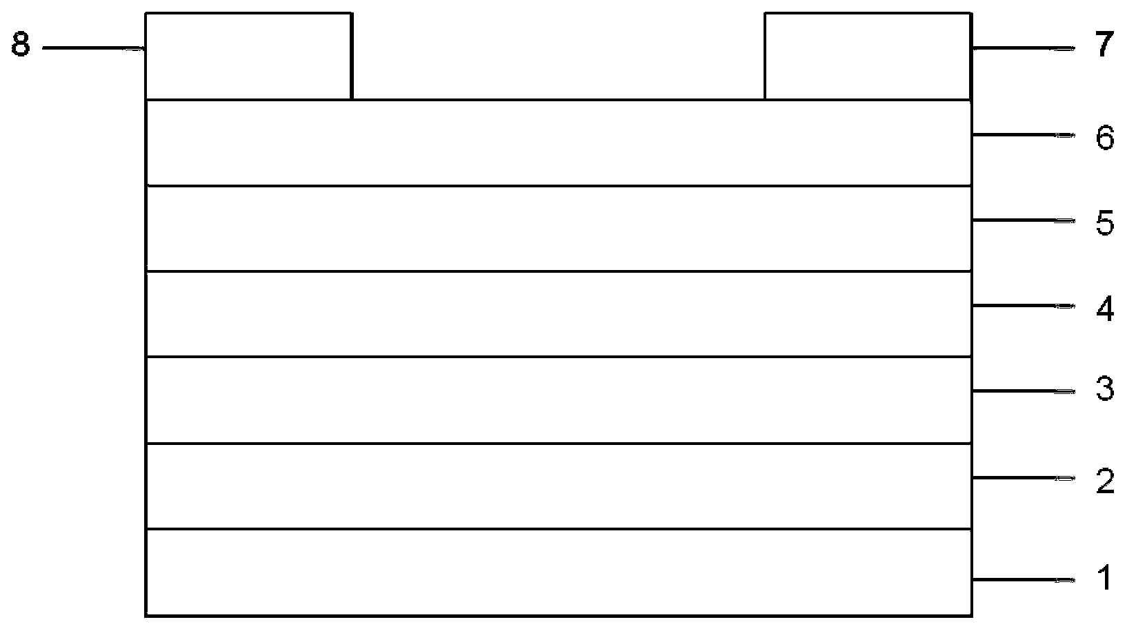
[0054] (1) In the organic thin film transistor-based transparent color-changing multiple anti-counterfeiting flash memory device of the present invention, the flexible substrate 1 is a polyimide (PI) transparent substrate with a thickness of 0.028mm, and the thickness of the flexible substrate can be adjusted according to the needs of the application depends. The cleaned flexible substrate 1 is placed in a drying oven to bake and dry.
[0055] (2) will be doped with europium oxide (Eu 2 o 3 ) of gadolinium oxide (Gd 2 o 3 ) under high vacuum (vacuum degree 5.0×10 -3 Pascal) deposited on the flexible substrate 1 by electron beam evaporation technique, the obtained Gd 2 o 3 :Eu 2 o 3 The thickness of the film was 100 nanometers, as the optical film 2.
[0056] (3) Prepare a PDMS film with a thickness of 300 nm on the optical film 2 by a solution spin coating method as the modification layer 3 .
[0057] (4) A PEDOT:PSS thin film is prepared on the modification layer 3 ...
Embodiment 2
[0063] (1) In the transparent color-changing multiple anti-counterfeiting flash memory device based on organic thin film transistors of the present invention, the flexible substrate 1 is a 0.1 mm thick polyethylene terephthalate (PET) film. The cleaned flexible substrate 1 is baked and dried in an oven.
[0064] (2) Incorporate DBR fragments into PS solution, where the low refractive index material of DBR is SiO 2 , the high refractive index material is TiO 2 , the number of cycles is 40. The film obtained by spin coating was used as the optical film 2, and the film thickness was 200 nm.
[0065] (3) Prepare a PI polymer film with a thickness of 200 nanometers on the optical film 2 by solution spin coating method as the modification layer 3 .
[0066] (4) Under high vacuum (vacuum degree 4.0×10 -2 Pascal) deposited ITO on the modification layer 3 by magnetron sputtering as the gate 4 . During the deposition process, the substrate temperature is 80°C, the thickness of the ...
Embodiment 3
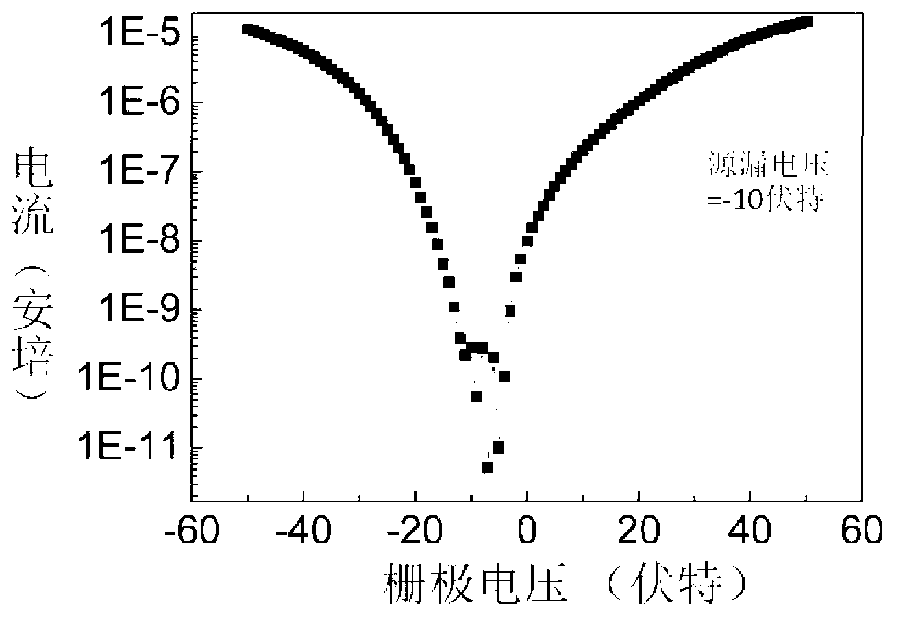
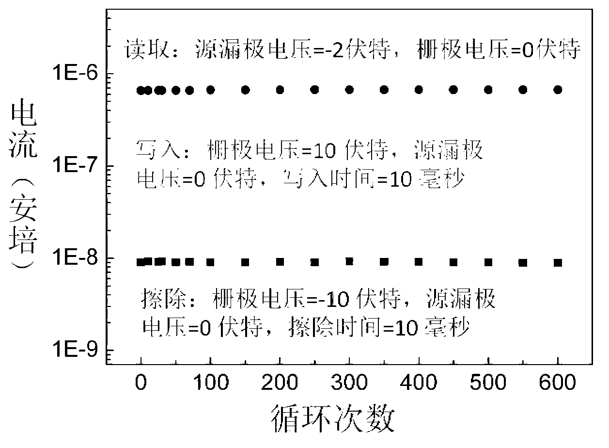
[0072] Referring to Example 1, the difference is that the optical film 2 is composed of two layers of films. First under high vacuum (vacuum degree 5.0×10 -3 Pascal) doped with europium oxide (Eu 2 o 3 ) Zirconia (ZrO 2 :Eu 2 o 3 )film. Incorporate DBR fragments into PS solution, where the low refractive index material of DBR is SiO 2 , the high refractive index material is Ta 2 o 5 , the number of cycles is 38. Then, the PS solution mixed with DBR fragments was used to form a film on ZrO by solution spin coating. 2 :Eu 2 o 3 On the film, a double-layer film is finally formed to form the optical film 2 together. All the other steps are the same as in Example 1. The device in Example 3 has good portability, transparency, and memory properties, and simultaneously has photoluminescent and optically variable anti-counterfeiting properties.
PUM
 Abstract
Description
Claims
Application Information