A kind of semiconductor structure and its forming method

A type of semiconductor technology, applied in the direction of semiconductor devices, semiconductor lasers, laser components, etc., can solve problems such as low symmetry and adverse effects on the optical characteristics of semiconductor devices, achieve uniform distribution, eliminate polarization effects, and improve utilization. Effect

Active Publication Date: 2016-08-03
BYD SEMICON CO LTD
View PDF10 Cites 0 Cited by
  • Summary
  • Abstract
  • Description
  • Claims
  • Application Information

AI Technical Summary

Problems solved by technology

Since the symmetry of the wurtzite structure material is relatively low, the wurtzite nitride material will generate spontaneous polarization and piezoelectric polarization inside, causing a strong built-in electric field (the intensity is on the order of several MV / cm), As a result, the optical properties of semiconductor devices based on wurtzite nitride heterojunctions are adversely affected; the two-dimensional quantum well structure only restricts the movement of carriers in two directions, so the quantum efficiency of the device may be further improved

Method used


Image

  • A kind of semiconductor structure and its forming method
  • A kind of semiconductor structure and its forming method
  • A kind of semiconductor structure and its forming method

Examples


Embodiment Construction

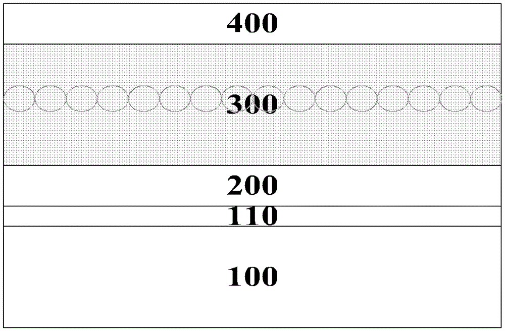
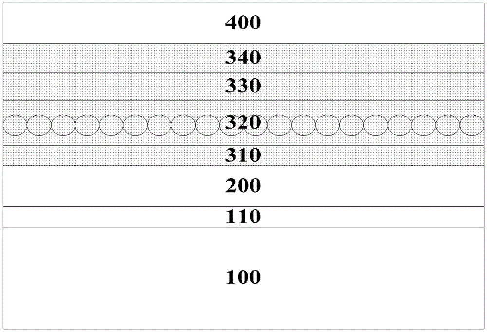
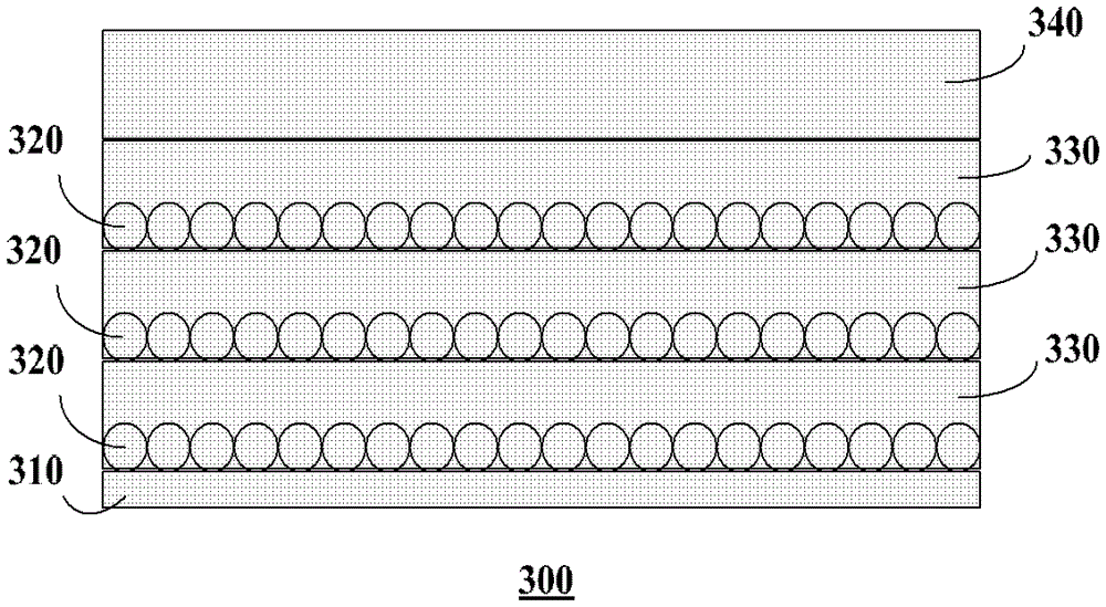
[0028] Embodiments of the present invention are described in detail below, examples of which are shown in the drawings, wherein the same or similar reference numerals designate the same or similar elements or elements having the same or similar functions throughout. The embodiments described below by referring to the figures are exemplary only for explaining the present invention and should not be construed as limiting the present invention.

[0029] In describing the present invention, it should be understood that the terms "longitudinal", "transverse", "upper", "lower", "front", "rear", "left", "right", "vertical", The orientation or positional relationship indicated by "horizontal", "top", "bottom", "inner", "outer", etc. are based on the orientation or positional relationship shown in the drawings, and are only for the convenience of describing the present invention and simplifying the description, rather than Nothing indicating or implying that a referenced device or elem...


PUM


Abstract

The invention provides a semiconductor structure and a forming method thereof. The semiconductor structure comprises a substrate, a buffering layer which is formed on the substrate, a first type nitride layer which is formed on the buffering layer, and a quantum dot structure which is formed on the first type nitride layer, wherein the quantum dot structure comprises blende InxGa (1-x) N quantum dot, wherein 0<=x<=1; and the semiconductor structure further comprises a second type nitride layer which is formed on the quantum dot structure. The semiconductor structure comprises the blende nitride quantum dot structure, eliminates a polarization effect and improves quantum efficiency.

Description

technical field [0001] The invention relates to the field of semiconductors, in particular to a semiconductor structure and a forming method thereof. Background technique [0002] In recent years, due to the wide application in optoelectronic devices such as high-brightness light-emitting diodes and laser diodes, the research on wide-bandgap nitride quantum structures based on InGaN / GaN semiconductor heterojunctions has attracted people's attention. The present experimental and theoretical results show that III-V nitrides usually grow into stable wurtzite structure and metastable sphalerite structure. Studies have also found that the optical properties of the wurtzite InGaN / GaN heterojunction are affected by a strong built-in electric field due to spontaneous and piezoelectric polarization, the strength of which is on the order of several MV / cm Magnitude. [0003] The essence of the quantum dot material is an atomic cluster, the size of which is on the order of nanometers,...

Claims


Application Information

Patent Timeline
Patent Type & Authority Patents(China)
IPC IPC(8): H01L33/06H01L33/18H01L33/32H01L33/00H01S5/343
Inventor 陈飞
Owner BYD SEMICON CO LTD
Why Eureka
Try Eureka