LED structure using AlGaInN quaternary material as quantum well and quantum barrier and manufacturing method thereof
A technology of LED structure and quantum well, which is applied in the field of optoelectronics and can solve the problems of limiting the optional range of materials and reducing the optional range.
- Summary
- Abstract
- Description
- Claims
- Application Information
AI Technical Summary
Problems solved by technology
Method used
Image
Examples
Embodiment Construction
[0011] Technical scheme of the present invention is as follows:
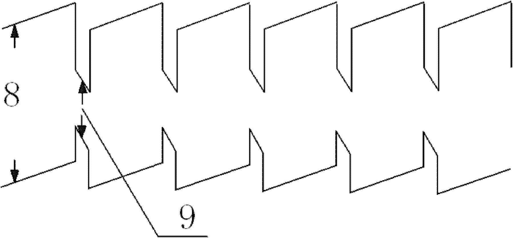
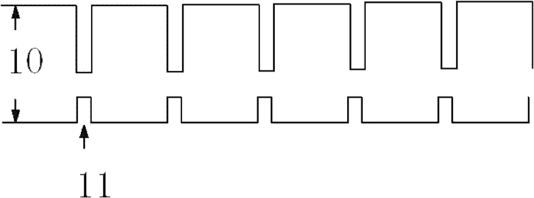
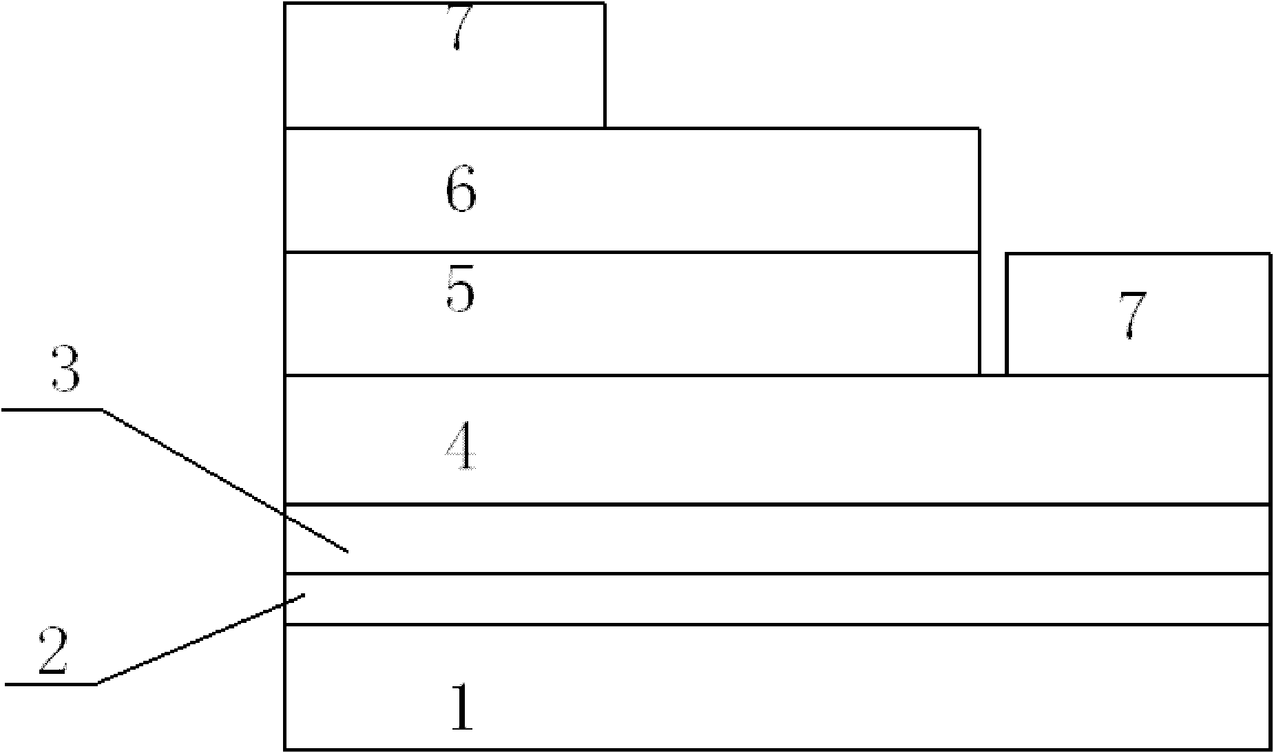
[0012] An LED structure using AlGaInN quaternary materials as quantum wells and quantum barriers, including a substrate layer followed by a nucleation layer, a buffer layer, an N-type conductive layer, a multi-quantum well layer and a P-type conductive layer, and on the N-type conductive layer On the top and on the P-type conductive layer are respectively ohmic contact layers; it is characterized in that the multiple quantum well layers are alternately grown Al with a thickness of 2-20nm x Ga 1-x-y In y N-well and Al with a thickness of 10-30nm u Ga 1-u-v In v N bases, the repetition period is 2-20, wherein, 0<x<1, 0<y<1; 0<u<1, 0<v<1.
[0013] The substrate layer is one of sapphire substrate or silicon carbide substrate.
[0014] The buffer layer is non-doped GaN with a thickness of 1 μm-100 μm, and the nucleation layer is GaN with a thickness of 10 nm-50 nm.
[0015] The N-type conductive layer is a Si-...
PUM
 Abstract
Description
Claims
Application Information


