Multi-line silicon wafer cutting method
A multi-wire cutting, silicon wafer technology, applied in fine working devices, stone processing equipment, manufacturing tools, etc., can solve the problems of parameter optimization, constraints, gaps, etc., to improve the cutting quality and reduce the adverse effects of cutting. Effect
- Summary
- Abstract
- Description
- Claims
- Application Information
AI Technical Summary
Problems solved by technology
Method used
Image

Examples
Embodiment Construction
[0026] The invention provides a magnesium oxide protective film evaporation device for a plasma display screen, which realizes the uniform height of each support block on a support carrier, thereby reducing the cracking probability of the glass substrate during the evaporation process, and at the same time reducing the Display scrap rate.
[0027] The following will clearly and completely describe the technical solutions in the embodiments of the present invention with reference to the accompanying drawings in the embodiments of the present invention. Obviously, the described embodiments are only some, not all, embodiments of the present invention. Based on the embodiments of the present invention, all other embodiments obtained by persons of ordinary skill in the art without making creative efforts belong to the protection scope of the present invention.
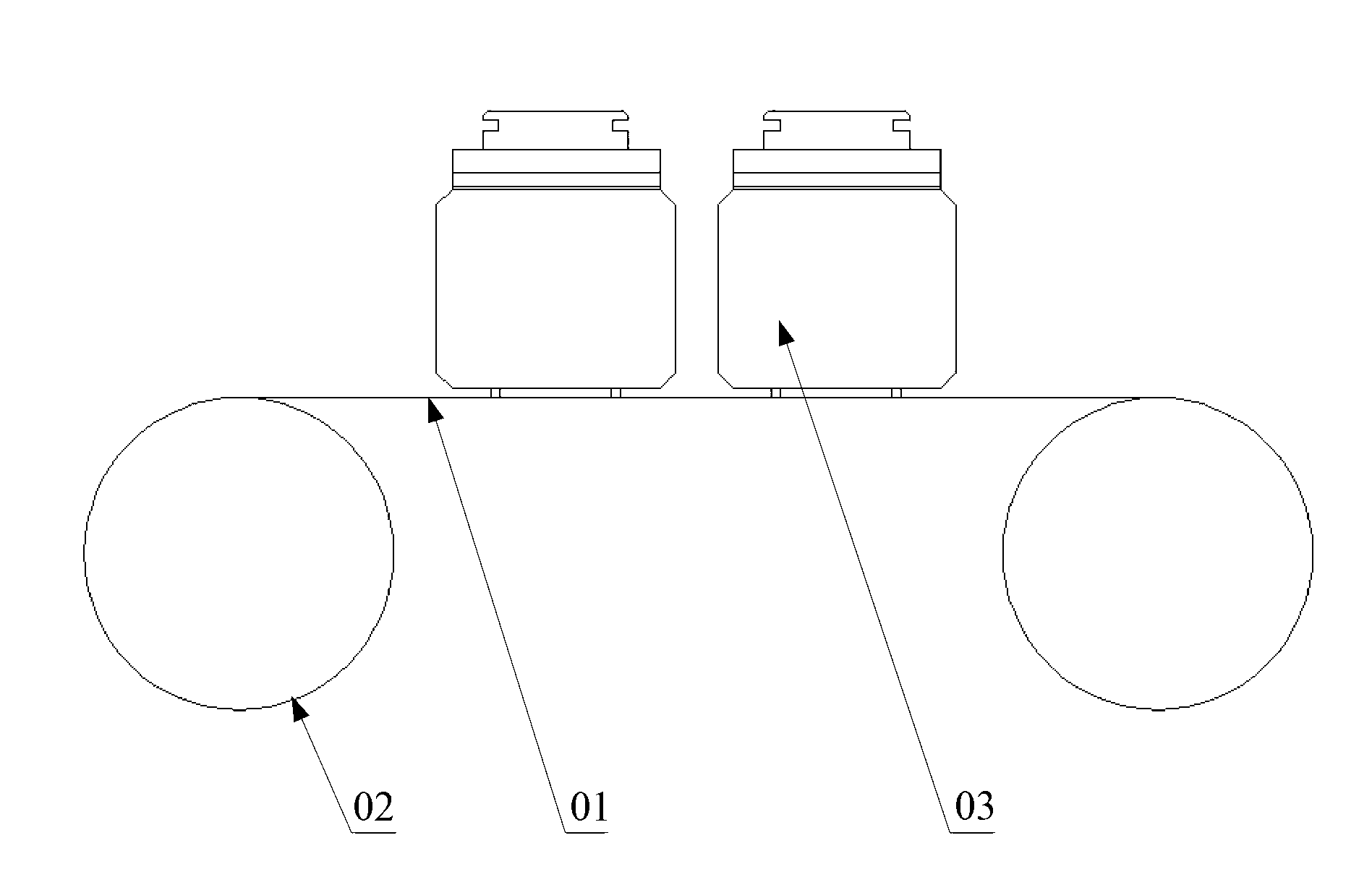
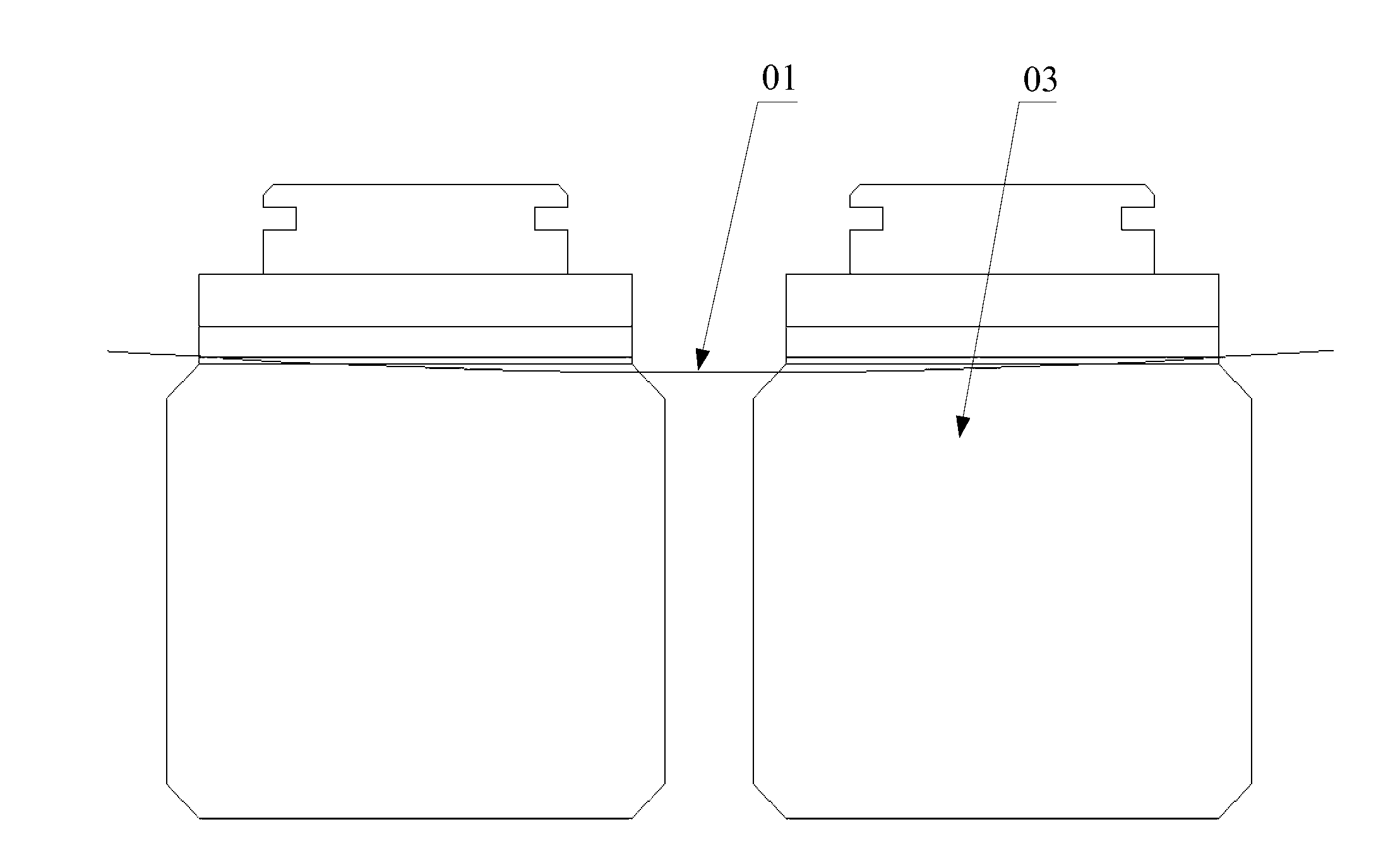
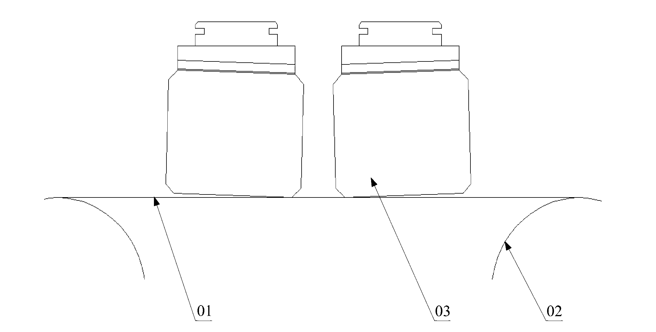
[0028] Such as Figure 4-Figure 7 As shown, the silicon wafer multi-wire cutting method provided by the embodiment of th...
PUM
 Abstract
Description
Claims
Application Information