Method for reducing packaging stress of micro-electromechanical system (MEMS) chip through back graphics

A chip packaging and patterning technology, applied in the photoengraving process of the pattern surface, the process for producing decorative surface effects, decorative arts, etc., can solve the problem that the size of the glue point cannot be accurately controlled, the MEMS chip 1 cannot be accurately positioned, Poor mechanical shock resistance

Inactive Publication Date: 2013-07-10
ANHUI BEIFANG XINDONG LIANKE MICROSYST TECH
View PDF12 Cites 24 Cited by
  • Summary
  • Abstract
  • Description
  • Claims
  • Application Information

AI Technical Summary

Problems solved by technology

But there are two disadvantages: one is that the contact area between the MEMS chip 1 and the glue 8 is small, and the mechanical impact resistance is poor; Moreover, the position of the MEMS chip 1 cannot be accurately positioned relative to the adhesive 8, and the packaging stress will be unevenly transmitted to the MEMS chip.
But there are also two disadvantages: one is that the contact area between the MEMS chip 1 and the adhesive 8 is small, and the resistance to mechanical shock is poor; conduction to the MEMS chip

Method used


Image

  • Method for reducing packaging stress of micro-electromechanical system (MEMS) chip through back graphics
  • Method for reducing packaging stress of micro-electromechanical system (MEMS) chip through back graphics
  • Method for reducing packaging stress of micro-electromechanical system (MEMS) chip through back graphics

Examples


Embodiment 1

[0032] The method of reducing the stress of MEMS chip packaging through back patterning, the specific steps are:

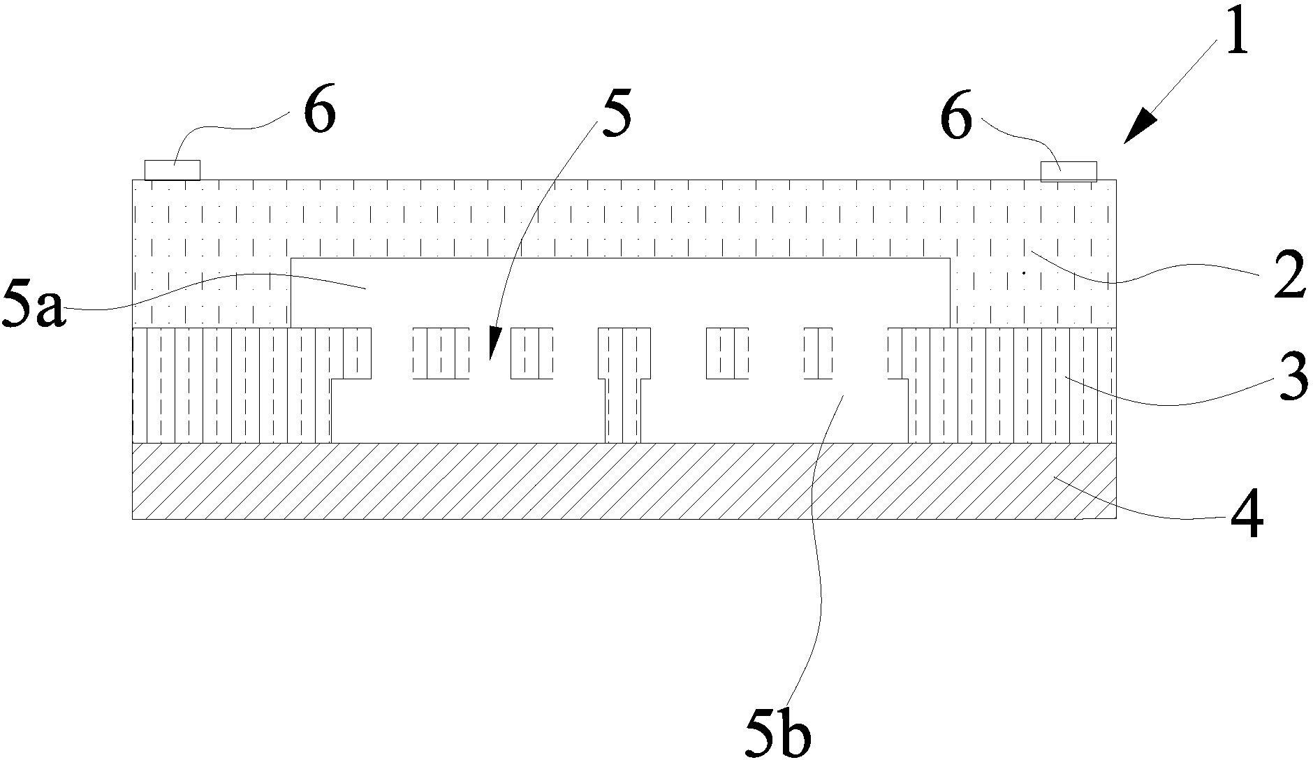
[0033] (1) will be as figure 1 The shown MEMS chip 1 without the package stress reduction structure is placed with its back facing up, and a photoresist 13 is coated on the back layer 4, as Figure 5 shown;

[0034] (2) Use a photolithography machine aligned on both sides to expose and develop the photoresist 13, and form a photoresist pattern 13' on the back layer 4, such as Image 6 shown;

[0035] (3) Perform dry etching on the back layer 4 of the MEMS chip 1 with the photoresist pattern 13' as an etching mask, control the etching parameters, and form the mounting column 14, the MEMS chip 1' with the mounting column 14 and the substrate Etch a thin backside layer 4', such as Figure 7 shown;

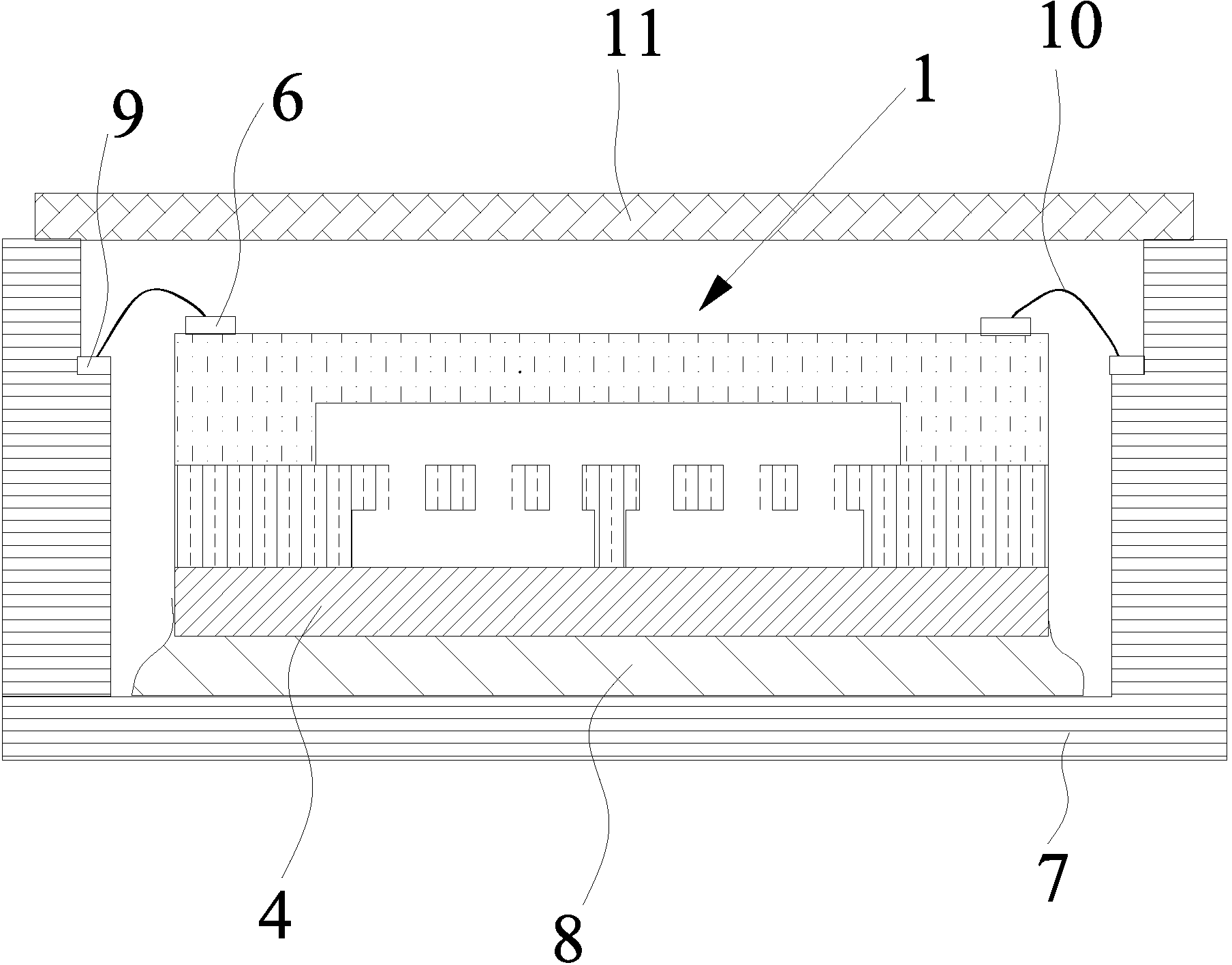
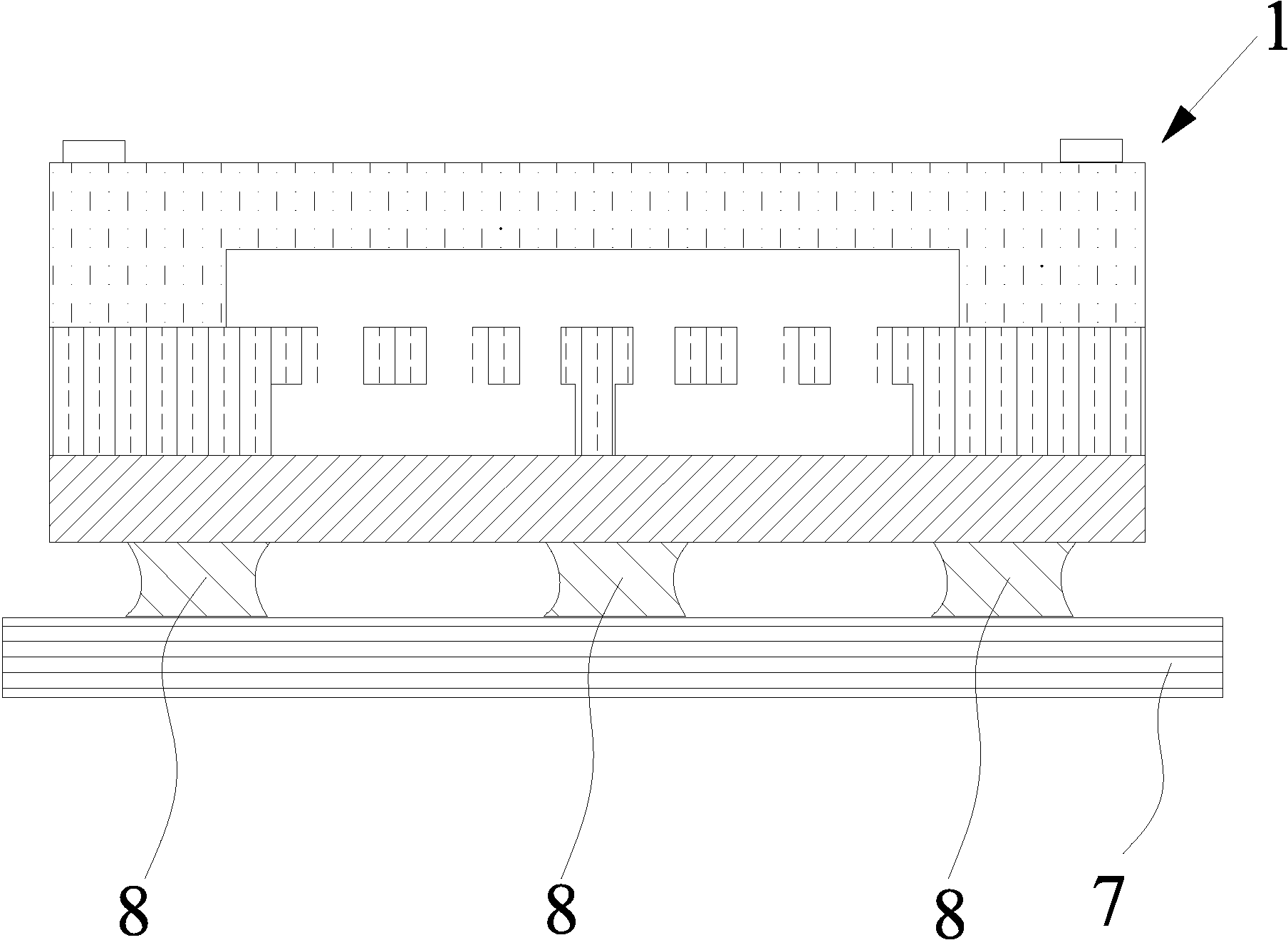
[0036] (4) Adhesive glue 8 is applied to the local point of the bottom plate of the packaging tube shell 7, and the MEMS chip 1′ with the chip mounting column 14 is ...

Embodiment 2

[0039] The difference between the second embodiment and the first embodiment is only that in step (4) the adhesive 8 is filled on the bottom plate of the package shell 7, and the MEMS chip 1' with the mounting post 14 is fixed on the package via the mounting post 14. The bottom plate of the tube shell 7, such as Figure 10 As shown, the adhesive film adhesive 8 has sufficient affinity with the film loading column 14, and the adhesive film adhesive 8 can move upwards along the film loading column 14. The pillars 14 are fully enclosed, thereby maintaining resistance to mechanical shock while reducing stress on the package.

Embodiment 3

[0041] The difference between Embodiment 3 and Embodiment 1 is that in step (3), during the etching process of the loading column, the ratio of deposition and etching atmospheres is alternately changed, and serrations are etched on the outer surface of the loading column to form a zigzag loading column. 14′, such as Figure 11 As shown, the surface area of ​​the sawtooth-shaped film loading column 14' is relatively large, and the contact area with the film adhesive 8 is also relatively large, so the mechanical shock resistance is relatively strong, but the area of ​​the sawtooth-shaped film loading column 14' in the horizontal direction The cross-sectional area of ​​the mounting post 14 is the same as that of the first and second embodiments, so the packaging stress is not much different from that of the first and second embodiments.


PUM


Abstract

The invention discloses a method for reducing the packaging stress of a micro-electromechanical system (MEMS) chip through back graphics. The method comprises the following specific steps of: coating photoresist on a back layer of the MEMS chip; exposing and developing the photoresist to form a photoresist graph on the back layer; etching the back layer of the MEMS chip by taking the photoresist graph as an etching mask to form chip mounting columns; coating a chip adhesive on a bottom plate of a packaging pipe shell, and fixing the MEMS chip with the chip mounting columns on the bottom plate of the packaging pipe shell through the chip mounting columns; after solidification, electrically connecting a pressure welding block of the MEMS chip with a metal welding block on the side surface of the packaging pipe shell by a wire; and covering a packaging cover plate. According to the method, the contact area between the MEMS chip and the bottom plate of the packaging pipe shell in the horizontal direction is reduced, and the surface area of the chip mounting columns is enlarged, so that enough contact area between the MEMS chip and the chip adhesive is ensured, the packaging stress is reduced, and the mechanical shock resistance is ensured.

Description

technical field [0001] The invention belongs to the technical field of chip packaging, and in particular relates to a method for reducing the stress of MEMS chip packaging through back patterning. Background technique [0002] Electronic packaging is to electrically connect one or more electronic component chips to each other, and then encapsulate them in a protective structure. Its purpose is to provide electrical connection, mechanical protection, chemical corrosion protection, etc. for electronic chips. Commonly used MEMS chips without packaging stress-reducing structures, such as figure 1 As shown, the MEMS chip 1 is composed of a front layer 2, a MEMS structure layer 3 and a back layer 4 through a wafer bonding process. There is at least one upper cavity 5a on the front layer 2, and at least one lower cavity on the MEMS structure layer 3. 5b, the upper and lower cavities and the MEMS structure layer 3 form a sealed cavity 5, which provides a closed space for free movem...

Claims


Application Information

Patent Timeline
Patent Type & Authority Applications(China)
IPC IPC(8): B81C1/00B81C3/00
Inventor 华亚平
Owner ANHUI BEIFANG XINDONG LIANKE MICROSYST TECH
Why Eureka
Try Eureka