Indium antimonide (InSb) wafer and silicon (Si) wafer bonding method

A wafer bonding and wafer technology, applied in the direction of sustainable manufacturing/processing, electrical components, climate sustainability, etc., can solve the problems of poor practicability, complex processes of InSb wafers and Si wafers, and achieve strong practicability and simple process Effect

Inactive Publication Date: 2013-07-10
INST OF SEMICONDUCTORS - CHINESE ACAD OF SCI
View PDF4 Cites 5 Cited by
  • Summary
  • Abstract
  • Description
  • Claims
  • Application Information

AI Technical Summary

Problems solved by technology

[0005] However, in the process of realizing the present invention, the applicant found that the processes of the existing InSb wafer and Si wafer bonding methods are very complicated and have poor practicability

Method used


Image

  • Indium antimonide (InSb) wafer and silicon (Si) wafer bonding method
  • Indium antimonide (InSb) wafer and silicon (Si) wafer bonding method
  • Indium antimonide (InSb) wafer and silicon (Si) wafer bonding method

Examples


Embodiment Construction

[0018] In order to make the object, technical solution and advantages of the present invention clearer, the present invention will be described in further detail below in conjunction with specific embodiments and with reference to the accompanying drawings. It should be noted that, in the drawings or descriptions of the specification, similar or identical parts all use the same figure numbers. Implementations not shown or described in the accompanying drawings are forms known to those of ordinary skill in the art. Additionally, while illustrations of parameters including particular values ​​may be provided herein, it should be understood that the parameters need not be exactly equal to the corresponding values, but rather may approximate the corresponding values ​​within acceptable error margins or design constraints.

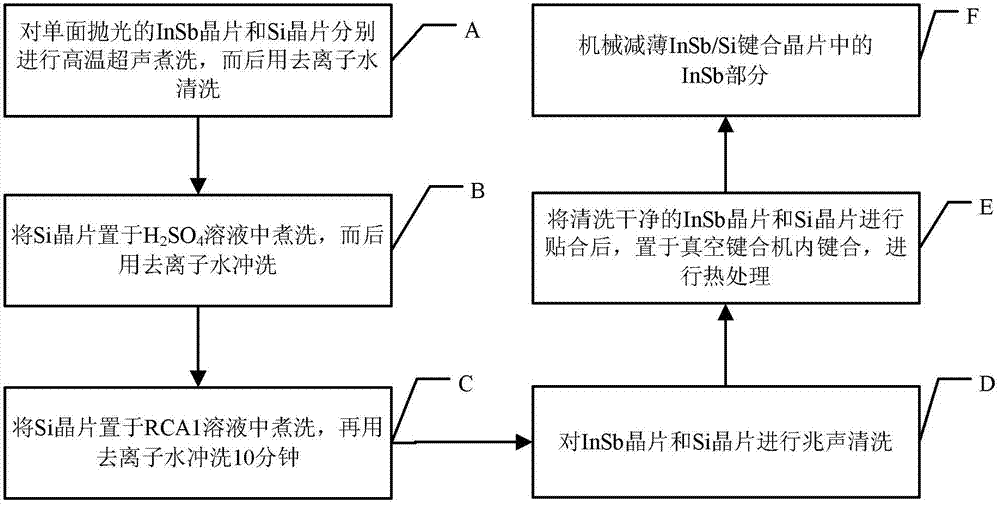
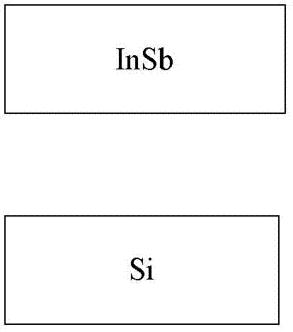
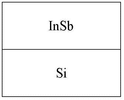
[0019] The invention proposes a new method for realizing the bonding of InSb and Si, which can be applied to InSb FPA detectors.

[0020] In an exemplary embo...


PUM


Abstract

The invention provides an indium antimonide (InSb) wafer and silicon (Si) wafer bonding method. The method includes a first step of carrying out high-temperature ultrasonic boiling and washing in organic solvent on an InSb wafer and a Si wafer which are respectively polished on at least one side and then using deionized water to wash the InSb wafer and the Si wafer, a second step of placing the Si wafer into acid solution for boiling and washing and then using the deionized water to wash, a third step of placing the Si wafer into alkali solution for boiling and washing and then using the deionized water to wash, and a fourth step of enabling the polished surface of the InSb wafer and the polished surface of the Si wafer to face inwards, carrying out laminating, then placing the two laminated wafers into a vacuum bonding machine and carrying out heat treatment to complete bonding of the InSb wafer and the Si wafer. The InSb wafer and Si wafer bonding method is simple in process and has strong practicality.

Description

technical field [0001] The invention relates to the technical field of growth of lattice-mismatched heterojunction materials in the semiconductor industry, in particular to a method for bonding InSb wafers and Si wafers that can be widely used in infrared focal plane technology. Background technique [0002] The development of infrared focal plane detectors, especially indium antimonide (InSb) infrared focal plane array (FPA) detectors in the mid-wave band, is relatively mature, and has been widely used in the fields of infrared guidance, tracking, and staring imaging weapons and equipment. Indium antimonide (InSb) infrared focal plane array (FPA) detector system is formed by flip-chip interconnection of InSb pixel array and Si readout circuit. Stress is introduced after the InSb pixel array is flip-chip interconnected with the Si readout circuit. When the strain exceeds the bearing capacity of InSb, it will be broken. At the same time, the strain will also reduce the perfor...

Claims


Application Information

Patent Timeline
Patent Type & Authority Applications(China)
IPC IPC(8): H01L31/18
CPCY02P70/50
Inventor 彭红玲郑婉华
Owner INST OF SEMICONDUCTORS - CHINESE ACAD OF SCI
Why Eureka
Try Eureka