Mode add-drop multiplexing and demultiplexing device based on grating-assisting type coupler

A demultiplexer and coupler technology, which is applied in the field of mode multiplexing and demultiplexing, can solve the problem of difficult realization of more than three mode channels, increased device design complexity, and small device process tolerance. problems, to achieve the effect of easy integration and expansion, compact size, convenient and low-cost manufacturing

Inactive Publication Date: 2013-07-24
ZHEJIANG UNIV
View PDF3 Cites 30 Cited by
  • Summary
  • Abstract
  • Description
  • Claims
  • Application Information

AI Technical Summary

Problems solved by technology

The former is difficult to achieve more than three mode channels, and the process tolerance of the device is small, so it is not easy to manufacture; the latter requires strict coupling length, and also needs to adjust the width of the bus multimode waveguide, which increases the complexity of device design

Method used


Image

  • Mode add-drop multiplexing and demultiplexing device based on grating-assisting type coupler
  • Mode add-drop multiplexing and demultiplexing device based on grating-assisting type coupler
  • Mode add-drop multiplexing and demultiplexing device based on grating-assisting type coupler

Examples


Embodiment 1

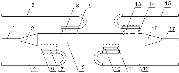
[0038] like figure 1 , Figure 5 and Image 6 As shown, the silicon-on-insulator (SOI) material with a top silicon thickness of 220 nm and a silicon oxide buried layer of 2 μm is used. The silicon strip waveguide with a width of 450 nm and a width of 1.1 um was fabricated by dry silicon etching, and the waveguide interval was 400 nm. A Bragg waveguide grating is etched in the center of the waveguide. The width of the rectangular grating teeth is 200 nm, and its period is 314 nm in the upper coupling region 6 and lower coupling region 11, and 347 nm in the upper coupling region 9 and lower coupling region 14. .

[0039] The grating period parameters in the above embodiments are designed for the device working in TE mode, and the device can also work in TM mode, only need to change different grating period parameters. The entire device only needs to be etched once to complete the fabrication.

Embodiment 2

[0041] like figure 1 , Figure 5 and Figure 7 As shown, the silicon-on-insulator (SOI) material with a top silicon thickness of 220 nm and a silicon oxide buried layer of 2 μm is used. The silicon ridge waveguide with a width of 450 nm and a width of 1.1 um was produced by twice dry silicon etching, with a ridge height of 160 nm and a waveguide interval of 400 nm. Bragg waveguide gratings are etched on the outer ridge in the center of the waveguide. The teeth of the rectangular grating are 200 nm, and its period is 308 nm in the upper coupling region 6 and the lower coupling region 11, and in the upper coupling region 9 and lower coupling region 14. 338 nm.

[0042] The grating period parameters in the above embodiments are designed for the device working in TE mode, and the device can also work in TM mode, only need to change different grating period parameters. The entire device only needs to be etched twice to complete the fabrication.


PUM


Abstract

The invention discloses a mode add-drop multiplexing and demultiplexing device based on a grating-assisting type coupler. The device comprises three add single-mode waveguides, an add mode converter, a bus multi-mode waveguide, two add Bragg waveguide gratings, a drop mode converter, three drop single-mode waveguides, two drop Bragg waveguide gratings, two add coupling areas and two drop coupling areas. The Bragg waveguide gratings are arranged between the bus multi-mode waveguide and the add and drop single-mode waveguides, and the energy exchange between the multi-mode waveguide and the single-mode waveguides is realized due to the micro-interference function of the refraction rate. The device has the advantages that the coupling is realized between the single-mode waveguides and the multi-mode waveguide in different modes; the coupling coefficient is adjustable, the bandwidth is large, the number of information carrying channels is multiple, and the like; the design structure is simple, and the size is compact; the device manufacturing process is compatible with a CMOS (complementary metal oxide semiconductor) process, so the integration and the extension are easy, the low-cost manufacturing is convenient, and the device can be widely applied to the on-chip and high-density integrated type optical interconnection system.

Description

technical field [0001] The invention relates to an optical mode multiplexing and demultiplexing integrated device, in particular to a mode adding / dropping multiplexing and demultiplexing device based on a grating auxiliary coupler. Background technique [0002] With the continuous development of today's society, people's demand for high-capacity, large-bandwidth and integrated optical interconnection technology is imminent. It is the general trend to realize photoelectric hybrid integration on the same chip, and it is the best way to solve the current bottleneck of electrical interconnection. In order to increase the bandwidth capacity of optical communication and improve the integration of the system, people usually use the optical wavelength division multiplexing (WDM) technology. However, for on-chip optical interconnection technology, the more channels of wavelength division multiplexing, the more lasers need to be integrated on the chip, which will greatly increase the...

Claims


Application Information

Patent Timeline
Patent Type & Authority Applications(China)
IPC IPC(8): G02B6/12G02B6/124
Inventor 邱晖晔胡挺邵海峰金亿昌杨建义江晓清
Owner ZHEJIANG UNIV
Why Eureka
Try Eureka