Full-self-aligned insulated gate bipolar transistor device and manufacturing method thereof

A bipolar transistor, self-aligned technology, applied in semiconductor/solid-state device manufacturing, electrical components, circuits, etc., can solve problems such as hidden dangers of devices, unreasonable device structures, affecting device operating parameters and reliability, etc. , Reduced process steps, improved latch-up effect

Active Publication Date: 2013-07-24
中国东方电气集团有限公司 +1
View PDF4 Cites 6 Cited by
  • Summary
  • Abstract
  • Description
  • Claims
  • Application Information

AI Technical Summary

Problems solved by technology

[0013] In terms of production process, the existing technology adopts multiple photolithography and etching processes. Due to the problem of alignment accuracy in the photolithography machine itself, the width W of the window layer between the polycrystalline grids can only be limited to the width of the photolithography machine. Within the width that the precision can achieve, if the width W of the device window layer is further reduced, many hidden dangers will be brought to the device, and the device structure will be unreasonable, which will affect the working parameters and reliability of the device.

Method used


Image

  • Full-self-aligned insulated gate bipolar transistor device and manufacturing method thereof
  • Full-self-aligned insulated gate bipolar transistor device and manufacturing method thereof
  • Full-self-aligned insulated gate bipolar transistor device and manufacturing method thereof

Examples


Embodiment 1

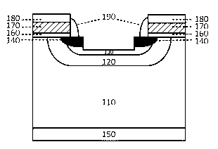
[0069] As shown in FIG. 1 , it is a fully self-aligned insulated gate bipolar transistor device, including a substrate 110 of a first conductivity type, and a substrate of a second conductivity type region 120, the second conductivity type base region 120 is provided with a second conductivity type deep diffusion region 130, the second conductivity type deep diffusion region 130 is in a "concave" shape, and the second conductivity type base region 120 is provided with a first Emitting regions 140 of conductivity type, the emitting regions 140 of the first conductivity type are respectively arranged on the two convex parts of the "concave" type of the deep diffusion region 130 of the second conductivity type, and the first main surface of each emitting region 140 of the first conductivity type A gate insulating layer 160 is provided, a polysilicon gate layer 170 is provided on the gate insulating layer 160, a second insulating layer 180 is provided on the polysilicon gate layer ...

Embodiment 2

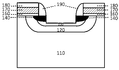
[0099] As shown in FIG. 1 , it is a fully self-aligned insulated gate bipolar transistor device, including a substrate 110 of a first conductivity type, and a substrate of a second conductivity type region 120, the second conductivity type base region 120 is provided with a second conductivity type deep diffusion region 130, the second conductivity type deep diffusion region 130 is in a "concave" shape, and the second conductivity type base region 120 is provided with a first Emitting regions 140 of conductivity type, the emitting regions 140 of the first conductivity type are respectively arranged on the two convex parts of the "concave" type of the deep diffusion region 130 of the second conductivity type, and the first main surface of each emitting region 140 of the first conductivity type A gate insulating layer 160 is provided, a polysilicon gate layer 170 is provided on the gate insulating layer 160, a second insulating layer 180 is provided on the polysilicon gate layer ...

Embodiment 3

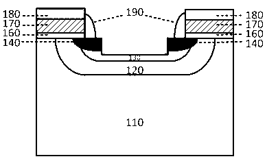
[0101] As shown in FIG. 1 , it is a fully self-aligned insulated gate bipolar transistor device, including a substrate 110 of a first conductivity type, and a substrate of a second conductivity type region 120, the second conductivity type base region 120 is provided with a second conductivity type deep diffusion region 130, the second conductivity type deep diffusion region 130 is in a "concave" shape, and the second conductivity type base region 120 is provided with a first Emitting regions 140 of conductivity type, the emitting regions 140 of the first conductivity type are respectively arranged on the two convex parts of the "concave" type of the deep diffusion region 130 of the second conductivity type, and the first main surface of each emitting region 140 of the first conductivity type A gate insulating layer 160 is provided, a polysilicon gate layer 170 is provided on the gate insulating layer 160, a second insulating layer 180 is provided on the polysilicon gate layer ...


PUM


Abstract

The invention relates to a semiconductor device in the field of power electronics, and in particular relates to a full-self-aligned insulated gate bipolar transistor device and a manufacturing method thereof. The device comprises a first conduction type substrate, and is characterized in that a second conduction type base region is formed in a first primary plane of the first conduction type substrate; and a second conduction type deep diffusion region is formed in the second conduction type base region and is in the shape of a Chinese character 'ao' meaning concave. The bipolar transistor device adopts insulated side walls and a technology of full self alignment, photolithography is not needed, the width of a polysilicon window can be reduced to 4 microns and even 2 microns, and thus more refined patterns can be achieved.

Description

technical field [0001] The semiconductor device of the present invention relates to the technical field of power electronics, specifically a fully self-aligned insulated gate bipolar transistor device and a manufacturing method thereof. Background technique [0002] The existing insulated gate bipolar transistor IGBT is mainly composed of N-drift region, P body region, deep P+ region, N+ emitter region, P+ collector region, SiO2 gate oxide layer, polysilicon gate layer, SiO2 oxide layer (including SiO2 layer, PSG phosphosilicate glass layer, SiO2 layer), front metal layer and back metal layer. The front metal layer is in contact with the P body region and the N+ emitter region at the same time, forming the emitter of the device. The backside metal contacts the P+ collector region, which constitutes the collector of the device. The polysilicon gate together with the attached metal forms the device gate. [0003] As shown in Figure 2, the IGBT device can be divided into a P...

Claims


Application Information

Patent Timeline
Patent Type & Authority Applications(China)
IPC IPC(8): H01L21/331
Inventor 张世勇胡强樱井建弥
Owner 中国东方电气集团有限公司
Why Eureka
Try Eureka