Manufacturing method of palladium-plated gold-plated double-plating bonding copper wire

A technology for bonding copper wires and manufacturing methods, which is applied in semiconductor/solid-state device manufacturing, electrical components, electrical solid-state devices, etc., and can solve problems such as poor electrical conductivity and poor ductility

Inactive Publication Date: 2013-07-24
溧阳市虹翔机械制造有限公司
View PDF6 Cites 9 Cited by
  • Summary
  • Abstract
  • Description
  • Claims
  • Application Information

AI Technical Summary

Problems solved by technology

[0004] The technical problem to be solved by the present invention is to provide a double-coated bonding copper wire to overcome the defects of poor electrical conductivity and poor ductility of existing palladium-plated or silver-plated bonding copper wires

Method used


Image

  • Manufacturing method of palladium-plated gold-plated double-plating bonding copper wire

Examples


Embodiment

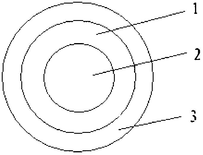
[0012] like figure 1 As shown, the double-coated bonding copper wire proposed by the present invention includes a copper core 1 , a palladium-plated layer 2 and a gold-plated layer 3 . Among them, the copper core 1 is made of high-purity copper with a purity greater than 99.9995% as a raw material, and is formed by adding tin, magnesium and aluminum for single crystal melting; Plated on the surface of the copper core; the gold-plated layer 3 is metal gold with a purity greater than 99.99%, which is electroplated on the surface of the palladium-plated layer 2 through an electroplating process. Wherein, based on 100 parts by weight of the final double-coated bonding copper wire containing palladium-plated layer and gold-plated layer, that is, 100wt%, the content of pure copper in the copper core is 92.6-93.8wt%, and the pure palladium conductive layer The content of the pure gold conductive layer is 2.7-5.4wt%, the content of the pure gold conductive layer is 1-2.5wt%, the cont...


PUM

PropertyMeasurementUnit
diameteraaaaaaaaaa

Abstract

The invention discloses a double-plating bonding copper wire of a three-layer structure. The innermost layer of the copper wire is a copper core formed due to the fact that trace metal elements are added to high-purity copper, the surface of the copper core is plated with a pure-palladium conductive layer, and the surface of the pure-palladium conductive layer is plated with a pure-gold conductive layer. The trace metal elements include tin, magnesium and aluminum.

Description

technical field [0001] The invention belongs to the field of semiconductor integrated circuit chip packaging, and in particular relates to a method for manufacturing a double-coated copper wire for semiconductor integrated circuit chip bonding. Background technique [0002] Although the chip obtained after the semiconductor integrated circuit is manufactured has a specific function, it must be connected with external electronic components to realize this function. The semiconductor integrated circuit chip needs to go through a bonding process with the package body, and finally get the chip package, so that it can be connected to external electronic components through the package pins. In the bonding process of the chip and the package, the bonding pads on the chip are electrically connected to the pins of the package through bonding wires. Therefore, the bonding wire is an essential material to realize the function of the chip. In the prior art, the Chinese authorized pate...

Claims


Application Information

Patent Timeline
Patent Type & Authority Applications(China)
IPC IPC(8): H01L21/48H01L23/49C22C9/02C25D5/10C25D3/44C25D3/50C25D5/50C21D8/06
CPCH01L24/45H01L2224/45664H01L2224/45644H01L2224/45572H01L2224/45147H01L24/43H01L2224/43H01L2224/4321H01L2224/43848H01L2224/45H01L2224/45015H01L2924/00014H01L2924/0105H01L2924/01012H01L2924/01013H01L2924/013H01L2924/00H01L2224/48H01L2924/20111H01L2924/00012H01L2924/01204H01L2924/01205
Inventor 吕燕翔居勤坤史仁龙万传友彭芳美周国忠
Owner 溧阳市虹翔机械制造有限公司
Why Eureka
Try Eureka