Thin film transistor and manufacturing method thereof and array substrate and display device

A technology for thin film transistors and substrates, which is applied in the fields of array substrates and display devices, thin film transistors and their manufacturing methods, can solve problems such as poor TFT performance, poor image quality, and poor Cu adhesion.

Active Publication Date: 2013-07-24
BOE TECH GRP CO LTD
View PDF6 Cites 29 Cited by
  • Summary
  • Abstract
  • Description
  • Claims
  • Application Information

AI Technical Summary

Problems solved by technology

[0004]The adhesion of Cu metal is relatively poor. The Cu process used in the TFT process generally requires the use of a buffer layer (Bufferlayer) to improve the adhesion of Cu. The common Bufferlayer can be molybdenum Mo , titanium Ti, Mo alloy, Ti alloy, etc., but the formed TFT has poor adhesion due to Cu, and the performance of TFT is poor, resulting in poor image quality

Method used


Image

  • Thin film transistor and manufacturing method thereof and array substrate and display device
  • Thin film transistor and manufacturing method thereof and array substrate and display device
  • Thin film transistor and manufacturing method thereof and array substrate and display device

Examples


Embodiment Construction

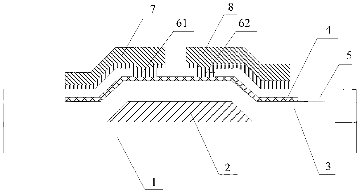
[0075] Embodiments of the present invention provide a thin film transistor and its manufacturing method, an array substrate and a display device, which are used to improve the performance of the TFT and improve the image quality.

[0076] The TFT provided by the embodiment of the present invention is preferably but not limited to be applicable to a display device under the planar electric field core technology, such as an ADS type display device. ADS is the core technology of planar electric field - Advanced Super Dimension Switch (ADS). Specifically, the electric field generated by the edge of the slit electrode (common electrode) in the same plane and the electric field generated between the slit electrode layer and the plate electrode layer (pixel electrode) form a multidimensional electric field, so that the slit electrodes in the liquid crystal cell, All aligned liquid crystal molecules directly above the electrodes can be rotated, thereby improving the working efficiency...


PUM


Abstract

The invention discloses a thin film transistor, a manufacturing method of the thin film transistor, an array substrate and a display device which are used for improving performance of the thin film transistor (TFT) and quality of an image. The thin film transistor comprises a substrate, a grid electrode formed on the substrate, a source electrode, a drain electrode, a semiconductor layer, a grid electrode insulation layer located between the grid electrode and the semiconductor layer or among the grid electrode, the source electrode and the drain electrode, an etching barrier layer located among the semiconductor layer, the source electrode and the drain electrode and provided with a source electrode contact hole and a drain electrode contact hole, a source electrode buffer layer located between the source electrode and the semiconductor layer and a drain electrode buffer layer located between the drain electrode and the semiconductor layer. The source electrode and the drain electrode are metallic copper electrodes. The buffer layers are made of copper alloy.

Description

technical field [0001] The invention relates to the field of display technology, in particular to a thin film transistor, a manufacturing method thereof, an array substrate and a display device. Background technique [0002] In the field of flat panel display technology, thin film transistor liquid crystal display (Thin Film Transistor Liquid Crystal Display, TFT-LCD) and organic electroluminescence display (Organic Light Emitting Display, OLED), because of its light, thin, low power consumption, high brightness , and the advantages of high image quality occupy an important position in the field of flat panel display. In particular, large-size, high-resolution, and high-quality flat panel display devices, such as liquid crystal televisions, have occupied a dominant position in the current flat panel display market. [0003] Currently, image signal delay is one of the key factors restricting large-size, high-resolution and high-quality flat panel display devices. Reducing t...

Claims


Application Information

Patent Timeline
Patent Type & Authority Applications(China)
IPC IPC(8): H01L29/786H01L29/417H01L21/336H01L21/28
CPCH01L21/28H01L29/786H01L29/45H01L29/78693H01L29/78618H01L21/441H01L27/1225H01L27/1259H01L29/66969H01L29/78606H01L29/7869H01L29/4908
Inventor 刘翔王刚薛建设
Owner BOE TECH GRP CO LTD
Why Eureka
Try Eureka