Method of manufacturing power transistor device

A technology of power transistor and manufacturing method, which is applied in the field of manufacturing power transistor components, can solve problems such as uneven distribution of hole concentration and electron concentration, achieve the effect of reducing surface doping concentration and improving withstand voltage capability

Inactive Publication Date: 2013-08-14
ANPEC ELECTRONICS CORPORATION
View PDF3 Cites 3 Cited by
  • Summary
  • Abstract
  • Description
  • Claims
  • Application Information

AI Technical Summary

Problems solved by technology

[0005] The main purpose of the present invention is to provide a method for reducing the surface doping concentration of the diffused doping region, a method for manufacturing a super junction structure, and a method for manufacturing power transistor components, so as to solve the problem of hole concentration and electron concentration distribution in the super junction structure uneven problem

Method used


Image

  • Method of manufacturing power transistor device
  • Method of manufacturing power transistor device
  • Method of manufacturing power transistor device

Examples


Embodiment Construction

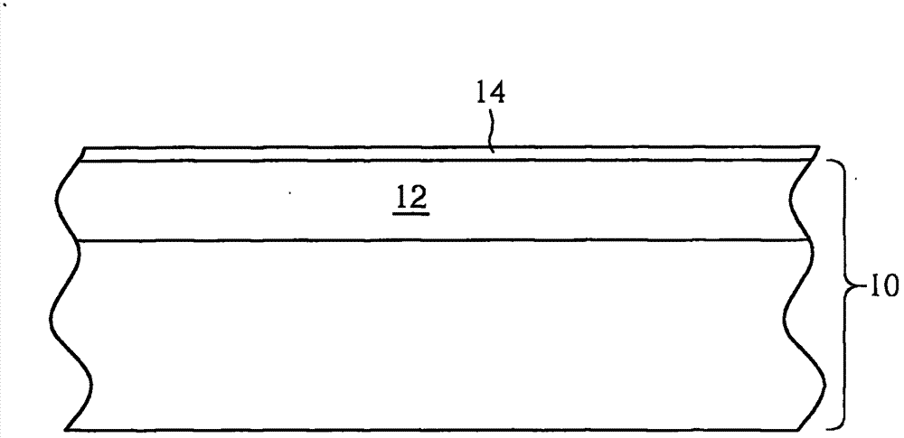
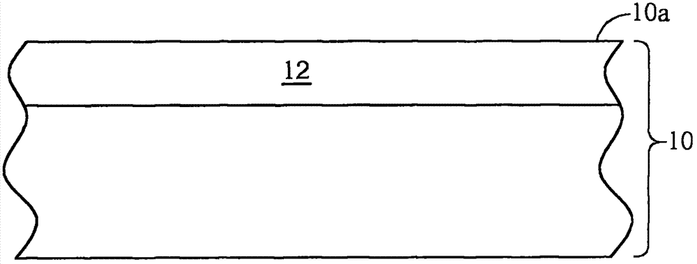
[0029] Please refer to Figure 1 to Figure 3 , Figure 1 to Figure 3 It is a schematic diagram of a method for reducing the surface doping concentration of a diffused doping region according to a preferred embodiment of the present invention. Such as figure 1 As shown, first, a semiconductor substrate 10, such as a silicon wafer, is provided. The semiconductor substrate 10 has a diffusion doping region 12 disposed therein, and the diffusion doping region 12 is in contact with an upper surface 10 a of the semiconductor substrate 10 . Moreover, the doping concentration of the diffused doping region 12 adjacent to the upper surface 10a is greater than the doping concentration of the diffused doping region 12 away from the upper surface 10a. Such as figure 2 As shown, subsequently, a thermal oxidation process is performed to form an oxide layer 14 on the upper surface 10 a of the semiconductor substrate 10 . Moreover, a part of the diffusion doped region 12 in contact with th...


PUM


Abstract

The present invention provides a method of manufacturing power transistor device. First, a semiconductor substrate is provided. The semiconductor substrate has the doped diffusion region disposed therein, and the doped diffusion region is in contact with a surface of the semiconductor substrate. A doping concentration of the doped diffusion region close to the surface is larger than a doping concentration of the doped diffusion region away from the surface. Then, a thermal oxidation process is performed to form an oxide layer on the surface of the semiconductor substrate. A part of the doped diffusion region in contact with the surface reacts with oxygen to form a part of the oxide layer. Then, the oxide layer is removed. Non-uniform concentration distribution of the hole carriers and the electrons in a super junction structure of the power transistor device can be overcome.

Description

technical field [0001] The invention relates to a manufacturing method of a power transistor assembly. Background technique [0002] In a power transistor component, the on-resistance RDS(on) between the drain and the source is proportional to the power consumption of the component, so reducing the on-resistance RDS(on) can reduce the power consumed by the power transistor component. In the on-resistance RDS(on), the resistance value caused by the epitaxial layer used for withstand voltage accounts for the highest proportion. Although increasing the doping concentration of conductive substances in the epitaxial layer can reduce the resistance value of the epitaxial layer, the function of the epitaxial layer is to withstand high voltage. If the doping concentration is increased, the breakdown voltage of the epitaxial layer will be reduced, thereby reducing the withstand voltage capability of the power transistor component. [0003] In order to maintain or improve the withst...

Claims


Application Information

Patent Timeline
Patent Type & Authority Applications(China)
IPC IPC(8): H01L21/336H01L21/02
CPCH01L21/30604H01L21/02238H01L29/7802H01L29/41766H01L29/0634H01L21/2255H01L29/456H01L29/0653H01L29/1095H01L29/66727
Inventor 林永发徐守一吴孟韦张家豪
Owner ANPEC ELECTRONICS CORPORATION
Why Eureka
Try Eureka