A method for reworking low square resistance silicon wafer after diffusion

A low-resistance, diffused technology, applied in sustainable manufacturing/processing, photovoltaic power generation, electrical components, etc., can solve the problems of high cost, complex process, long cycle, etc., to improve the square resistance, process time saving, photoelectricity The effect of improved conversion efficiency

Active Publication Date: 2016-06-01
CHINT NEW ENERGY TECH (HAINING) CO LTD
View PDF3 Cites 0 Cited by
  • Summary
  • Abstract
  • Description
  • Claims
  • Application Information

AI Technical Summary

Problems solved by technology

[0005] In order to solve the problem in the prior art that when the square resistance of the silicon wafer is low due to the abnormal diffusion process, it is necessary to rework from the texturing process, resulting in complex process, long cycle and high cost. A rework method for improving the square resistance of silicon wafers directly through diffusion

Method used


Image

  • A method for reworking low square resistance silicon wafer after diffusion
  • A method for reworking low square resistance silicon wafer after diffusion

Examples


Embodiment Construction

[0024] The following disclosure provides many different embodiments or examples for implementing different structures of the present invention. To simplify the disclosure of the present invention, components and arrangements of specific examples are described below. Furthermore, the present invention may repeat reference numerals and / or letters in different instances. This repetition is for the purpose of simplicity and clarity and does not in itself indicate a relationship between the various embodiments and / or arrangements discussed. It should be noted that components illustrated in the figures are not necessarily drawn to scale. Descriptions of well-known components and processing techniques and processes are omitted herein to avoid unnecessarily limiting the present invention.

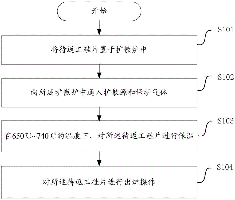
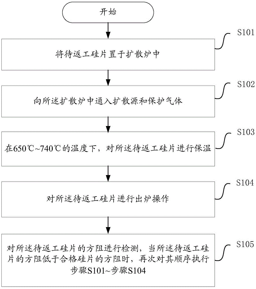
[0025] refer to figure 1 , figure 1 It is a schematic flowchart of a specific embodiment of a method for reworking a diffused low-resistivity silicon wafer according to the present invention. ...


PUM


Abstract

The invention discloses a low square resistance silicon chip reworking method after diffusion. The method comprises steps that: silicon chips to be reworked are placed in a diffusion furnace; protection gas is injected into the diffusion furnace; under the temperature of 650-740 DEG C, insulation treatment on the silicon chips to be reworked is carried out; and furnace outgoing operation of the silicon chips to be reworked is carried out. By employing the reworking method, reworking of the silicon chips having square resistance lower than a normal value is carried out to enable the square resistance to rise to a normal value. The method is advantaged in that: steps are simplified, operation technology is simple, reworking efficiency of the silicon chips having low square resistance can be substantially improved, and photoelectric conversion efficiency of subsequently-manufactured solar cells can further be substantially improved.

Description

technical field [0001] The invention belongs to the field of solar cell manufacturing, and in particular relates to a method for reworking low square resistance silicon wafers after diffusion. Background technique [0002] In crystalline silicon solar cells, the quality of the P-N junction directly affects the performance of the solar cell. Therefore, in the solar cell manufacturing process, the manufacture of the P-N junction has always been the focus of production. Diffusion junction plays a key role in the conversion efficiency of solar cells, and the diffusion process directly affects the quality of the P-N junction. [0003] In the process of preparing the P-N junction by diffusion, when the diffusion process is abnormal, the square resistance of the silicon wafer may be too small, resulting in a decrease in the photoelectric conversion efficiency of the subsequently prepared solar cell. Therefore, silicon wafers with too low resistance after diffusion can basically n...

Claims


Application Information

Patent Timeline
Patent Type & Authority Patents(China)
IPC IPC(8): H01L31/18
CPCH01L31/1804H01L31/1864Y02E10/547Y02P70/50
Inventor 李旺韩玮智牛新伟王仕鹏黄海燕陆川
Owner CHINT NEW ENERGY TECH (HAINING) CO LTD
Why Eureka
Try Eureka