A uniform diffusion control method for crystalline silicon solar cells
A solar cell, uniform diffusion technology, applied in the direction of circuits, electrical components, semiconductor devices, etc., can solve the problems of increasing the resistance of the moving current to the electrode of the grid line, the inability of the emitter to take into account at the same time, and the increase of the emitter resistance, etc., to reduce the surface Defects, improved life, and improved open-circuit voltage
- Summary
- Abstract
- Description
- Claims
- Application Information
AI Technical Summary
Problems solved by technology
Method used
Image
Examples
Embodiment 1
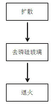
[0021] Select a single crystal silicon wafer; silicon wafer 1 undergoes a conventional cleaning process and texturing, puts silicon wafer 1 into a diffusion furnace, heats up to 805°C, and feeds large nitrogen (8L / min) and small nitrogen (1.5L / min) min), oxygen (0.8L / min) diffused for 12 minutes, and after the temperature was raised to 860 ° C, the diffusion junction was advanced for 5 minutes; the diffused silicon wafer was subjected to peripheral etching and phosphorus silicon glass removal; the obtained silicon wafer 1 was then placed in an oxidation furnace, Feed big nitrogen (7L / min), keep the temperature at 860°C for 5min. The square resistance of the silicon wafer obtained in Example 1 of the present invention is compared with the uniformity of the square resistance of the silicon wafer of the prior art, and the results are as follows:
[0022] .
Embodiment 2
[0024] Select a quasi-single crystal silicon wafer; silicon wafer 1 undergoes a conventional cleaning process and texturing, puts silicon wafer 1 into a diffusion furnace, heats up to 785°C, and feeds large nitrogen (6.5L / min), small nitrogen (1L / min), oxygen (0.25L / min) diffused for 15min, and after the temperature was raised to 830°C, the diffusion junction was advanced for 15min; the diffused silicon wafer 1 was placed in 5% hydrofluoric acid, and the reaction time was 50s; the obtained silicon wafer 1 Then put it into the oxidation furnace, feed large amount of nitrogen (7L / min), keep the temperature at 820°C for 10min. Comparing the battery sheet obtained in Example 2 of the present invention with the battery sheet of the prior art, the results are as follows:
[0025] .
PUM
 Abstract
Description
Claims
Application Information

