A method for fabricating a solar cell with an emitter structure with low, high and low doping concentrations

A solar cell, high and low doping technology, applied in circuits, electrical components, final product manufacturing, etc., can solve the problems of increasing the current resistance to the grid electrode, the inability of the emitter to take care of it at the same time, and the increase of the emitter resistance. The effect of reducing surface defects, improving life, and improving short-circuit current density

Active Publication Date: 2015-10-28
山东力诺太阳能电力股份有限公司
View PDF6 Cites 0 Cited by
  • Summary
  • Abstract
  • Description
  • Claims
  • Application Information

AI Technical Summary

Problems solved by technology

[0004] At present, the emitter made by the conventional diffusion method cannot meet the above two requirements at the same time
Generally, if the doping concentration is not too high, the Auger recombination will be greatly increased, and the minority carriers formed in the emission region are easy to recombine, resulting in a decrease in short-wave response; if the surface concentration is reduced, the junction depth will also become shallower, thin layer The resistance is high, and the resistance of the emitter must increase, thereby increasing the resistance of the current moving to the grid electrode in the emission area, increasing the probability of PN junction burn-through in the subsequent electrode sintering process, and reducing the battery yield.

Method used


Image

  • A method for fabricating a solar cell with an emitter structure with low, high and low doping concentrations

Examples


Embodiment 1

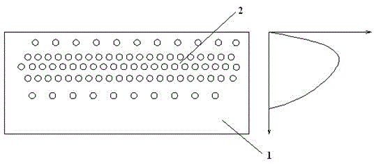
[0022] Select a single crystal silicon wafer; silicon wafer 1 undergoes a conventional cleaning process and texturing, puts silicon wafer 1 into a diffusion furnace, heats up to 805°C, and feeds large nitrogen (8L / min) and small nitrogen (1.5L / min) min), oxygen (0.8L / min) diffused for 12 minutes, and after the temperature was raised to 860 ° C, the diffusion junction was advanced for 5 minutes; the diffused silicon wafer was subjected to peripheral etching and phosphorus silicon glass removal; the obtained silicon wafer 1 was then placed in an oxidation furnace, Introduce large nitrogen (7L / min), keep the temperature at 860°C for 5min; use PECVD process to make a silicon nitride film on the surface of silicon wafer 1 with a thickness of 85nm and a refractive index of 2.08; then use screen printing and sintering in sequence , to obtain finished solar cells. Comparing the battery sheet obtained in Example 1 of the present invention with the battery sheet of the prior art, the re...

Embodiment 2

[0025] Select a quasi-single crystal silicon wafer; silicon wafer 1 undergoes a conventional cleaning process and texturing, puts silicon wafer 1 into a diffusion furnace, heats up to 785°C, and feeds large nitrogen (6.5L / min), small nitrogen (1L / min), oxygen (0.25L / min) diffused for 15min, and after the temperature was raised to 830°C, the diffusion junction was advanced for 15min; the diffused silicon wafer 1 was placed in 5% hydrofluoric acid, and the reaction time was 50s; the obtained silicon wafer 1 Put it into the oxidation furnace again, feed large nitrogen (7L / min), keep the temperature at 820°C, and the time is 10min; adopt the PECVD process to make a silicon nitride film on the surface of the silicon wafer 1 with a thickness of 75nm and a refractive index of 2.13; Screen printing and sintering are used in sequence to obtain finished solar cells. Comparing the battery sheet obtained in Example 2 of the present invention with the battery sheet of the prior art, the r...


PUM


Abstract

The invention relates to a solar cell manufacture method for an emitting electrode structure with low-high-low doping density. The method comprises a first step of manufacturing the surface of a silicon wafer after the felting process is carried out on the silicon wafer to an emitting electrode, a second step of etching the periphery of the silicon wafer obtained in the first step and removing phosphorosilicate glass, a third step of high temperature annealing of the silicon wafer obtained in the second step and a fourth step of carrying out a sedimentation silicon nitride, silk-screen positive and negative electrodes, back aluminum and sintering in sequence on the silicon wafer obtained in the third step. According to the solar cell manufacture method, uniformity of spreading sheet resistance can be effectively improved, microdefect and foreign ion in the silicon wafer are reduced through the high temperature annealing, lifetime of a minority carrier is prolonged, short-circuit current density is enabled to be increased by 0.1-1mA / cm2, open-circuit voltage is increased by 3-10mV, and conversion efficiency is increased by 0.1-0.5 %.

Description

technical field [0001] The invention relates to the technical field of solar cell fabrication, in particular to a solar cell fabrication method with an emitter structure of low, high, and low doping concentrations. Background technique [0002] Among all kinds of solar cells, crystalline silicon cells have always occupied the most important position. In recent years, great achievements and progress have been made in improving efficiency and reducing cost of crystalline silicon solar cells, further enhancing its dominant position in the future photovoltaic industry. [0003] As the core component of the solar cell, the emitter's surface doping concentration will directly affect the conversion efficiency of the solar cell. Solar cells have two requirements for the emitter: 1. The doping concentration should not be too high, and 2. The surface concentration should not be too low. [0004] At present, the emitter made by the conventional diffusion method cannot meet the above ...

Claims


Application Information

Patent Timeline
Patent Type & Authority Patents(China)
IPC IPC(8): H01L31/18
CPCY02P70/521Y02P70/50
Inventor 任现坤李秉霖姜言森张春艳程亮贾河顺徐振华
Owner 山东力诺太阳能电力股份有限公司
Why Eureka
Try Eureka