Silicon wafer surface topography reconstruction method based on B-spline

A technology of silicon wafer surface and spline surface, applied in image data processing, instrumentation, calculation, etc., can solve the problems of low responsiveness and low precision, achieve the effect of improving speed and precision, ensuring effective recovery, and eliminating burr phenomenon

Inactive Publication Date: 2013-09-11
INST OF OPTICS & ELECTRONICS - CHINESE ACAD OF SCI
View PDF3 Cites 9 Cited by
  • Summary
  • Abstract
  • Description
  • Claims
  • Application Information

AI Technical Summary

Problems solved by technology

[0007] The technical problem of the present invention is to overcome the shortcomings of low precision and low responsiveness in the prior art, and provide a method for reconstructing the surface topography of silicon wafers based on B-splines. The method ① has a high degree of fitting to the original appearance of silicon wafers and has Self-adaptive, satisfying overall fitting and local self-adaptiveness at the same time; ②The re

Method used


Image

  • Silicon wafer surface topography reconstruction method based on B-spline
  • Silicon wafer surface topography reconstruction method based on B-spline
  • Silicon wafer surface topography reconstruction method based on B-spline

Examples


Embodiment Construction

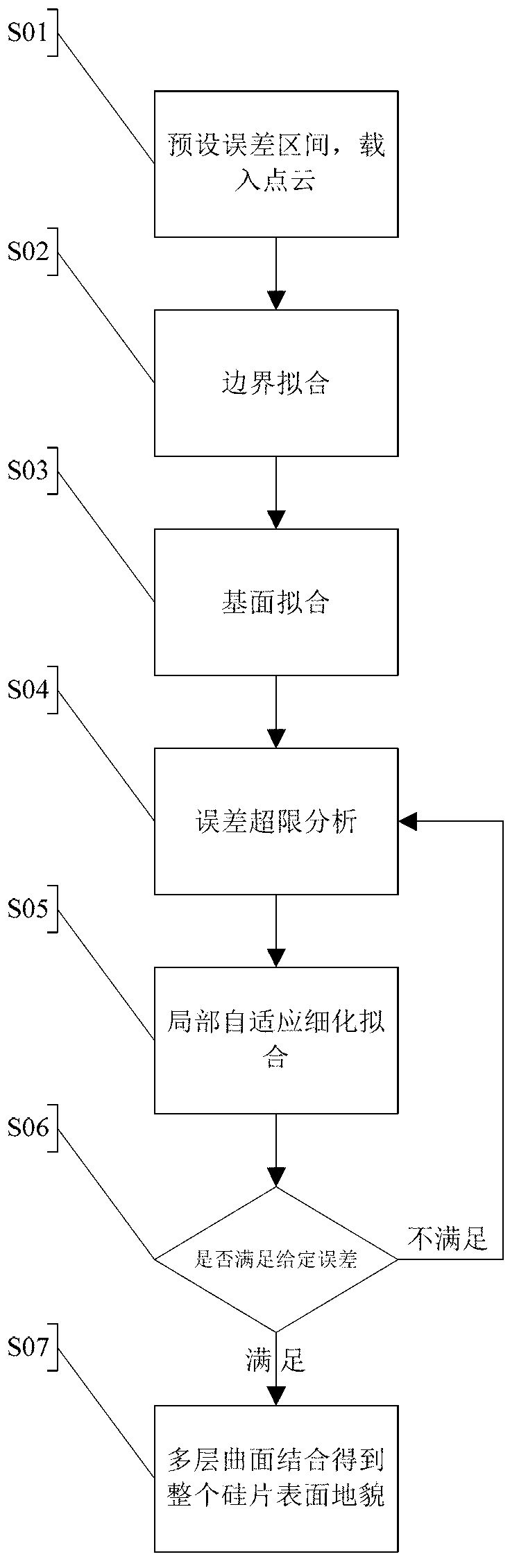
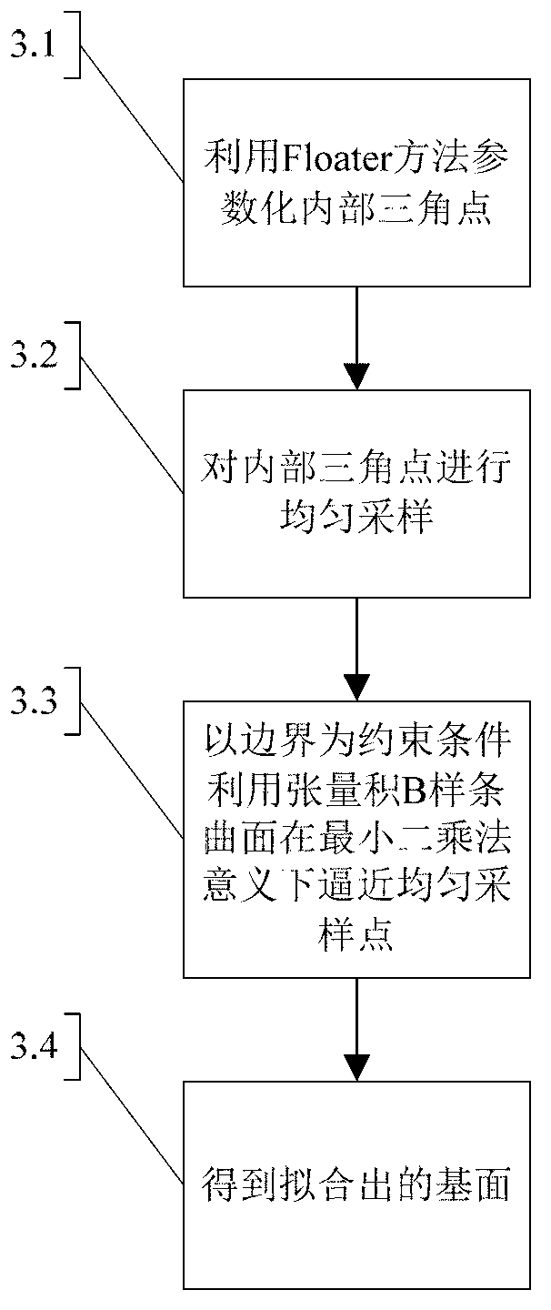
[0048] In order to make the purpose, technical solution and advantages of the present invention clearer, the overall algorithm flow of the present invention, the boundary synchronous fitting flow, the base surface fitting flow, and the local refinement fitting algorithm flow are described below in conjunction with the accompanying drawings and specific embodiments. Further introduction.

[0049] Such as figure 1 As shown, the overall algorithm flow is as follows:

[0050] Step S01: First preset the error interval ε 0 , and then load the point cloud of the surface topography of the silicon wafer, connect each point in the point cloud with two adjacent points, and triangulate the entire point cloud into triangular points;

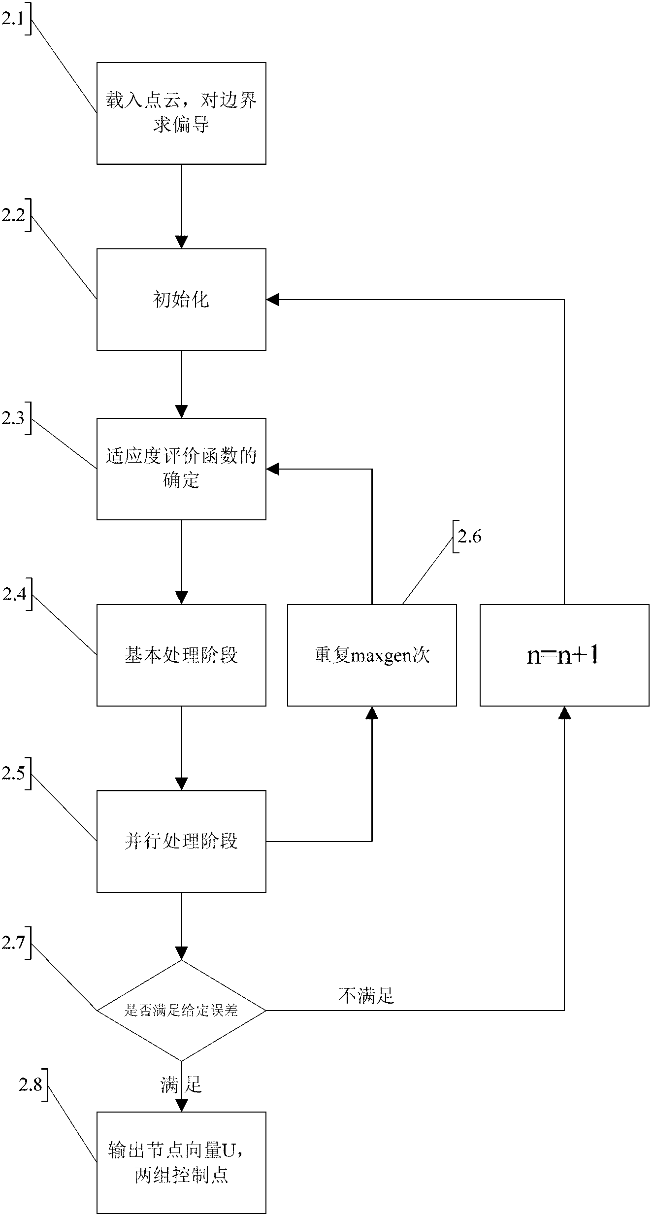
[0051] Step S02: Then parameterize the boundary points of the triangular mesh, and then use the genetic algorithm to perform two simultaneous boundary curve fittings on the boundary to obtain four B-spline boundary curves interpolated at the four corner poi...


PUM


Abstract

The invention provides a silicon wafer surface topography reconstruction method based on B-spline. The silicon wafer surface topography reconstruction method based on the B-spline comprises firstly fitting an input triangular mesh boundary, and then giving a boundary curve to perform surface fitting of an interpolation, and generating a first level B-spline surface; secondly, performing local adaptive refinement fitting on an error transfinite portion in an upper level B-spline surface and repeatedly performing local refinement fitting in this way until a given error is met; and finally, adding the multilevel B-spline surface with the offset to a base plane to obtain a fitting result. The silicon wafer surface topography reconstruction method based on the B-spline can simultaneously meet overall fitting and local adaptation of surface reconstruction, and effectively avoids data redundancy; and is strong in robustness and has significant effects for solving non-linear problems and restraining fuzzy noises; and the reconstructed surface is smooth and burr-free, so that the method can better meet response frequency requirements of actual motion of a motor.

Description

technical field [0001] The invention relates to a silicon chip surface topography reconstruction method, in particular to a silicon chip surface topography reconstruction method based on B-splines, which is applied to a focus detection system in a projection lithography system and belongs to the field of VLSI manufacturing and optics. The field of nano-device manufacturing and detection technology in microfabrication technology. Background technique [0002] The sharp improvement in the performance of lithography machines requires the use of larger numerical apertures and shorter wavelengths, resulting in a reduction in the depth of focus. The depth of focus of the widely used immersion lithography machine can only be maintained at the order of hundreds of nanometers, which has greatly exceeded the changes caused by vacuum adsorption warpage and substrate flatness, so it is required to improve the focus detection accuracy, and the silicon wafer Topography reconstruction is ...

Claims


Application Information

Patent Timeline
IPC IPC(8): G06T5/00
Inventor 王楠蒋薇严伟胡松
Owner INST OF OPTICS & ELECTRONICS - CHINESE ACAD OF SCI
Why Eureka
Try Eureka