Preparation method of silicon-based gallium arsenide material with low surface roughness

A silicon-based gallium arsenide, roughness technology, applied in chemical instruments and methods, from chemical reactive gases, semiconductor/solid-state device manufacturing, etc., can solve problems such as low surface roughness, and achieve the effect of low polishing rate

Active Publication Date: 2015-12-23
INST OF SEMICONDUCTORS - CHINESE ACAD OF SCI
View PDF4 Cites 0 Cited by
  • Summary
  • Abstract
  • Description
  • Claims
  • Application Information

AI Technical Summary

Problems solved by technology

[0007] The object of the present invention is to provide a method for preparing gallium arsenide-on-silicon material with low surface roughness to solve the problem of the transition from silicon substrate to III-V group material, and lay the foundation for GaAs-on-silicon optoelectronic and microelectronic devices. Substrate foundation

Method used


Image

  • Preparation method of silicon-based gallium arsenide material with low surface roughness
  • Preparation method of silicon-based gallium arsenide material with low surface roughness

Examples


Embodiment Construction

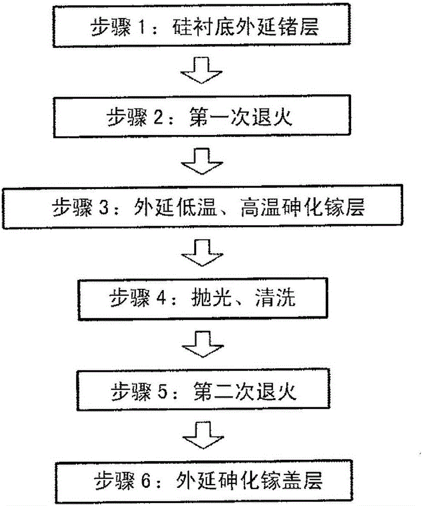
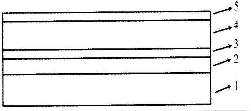
[0021] see figure 1 and figure 2 As shown, the present invention provides a method for preparing a silicon-based gallium arsenide material with low surface roughness, comprising the following steps:

[0022] Step 1: growing a germanium layer 2 on a silicon substrate 1 . This silicon substrate 1 is the (100) substrate of partial [011] direction 4 °, and size mainly depends on three equipments that need in this method: ultra-low vacuum chemical vapor phase epitaxy (UHVCVD), metal-organic chemical vapor deposition ( MOCVD) and polishing equipment, the size of the epitaxial wafers of the three equipments needs to be consistent, which can be 2 inches to 12 inches, or even larger; the growth of germanium layer 2 adopts UHVCVD, and the low-temperature germanium seed layer and the high-temperature germanium layer are cycled twice. technology, this step is a key step to obtain gallium arsenide, and the defect density of the germanium layer is required to be 1E5cm -2 Below, the roug...


PUM

PropertyMeasurementUnit
thicknessaaaaaaaaaa
surface roughnessaaaaaaaaaa

Abstract

The invention discloses a preparation method for silica-based gallium arsenide material with high quality and low surface roughness. The preparation method comprises the following steps: step 1, a germanium layer is grown on a silicon substrate; step 2, the silicon substrate on which the germanium layer is grown is placed in an MOCVD (metal-organic chemical vapor deposition) reaction chamber to be subjected to annealing for the first time; step 3, a low-temperature gallium arsenide nucleating layer and a high-temperature gallium arsenide layer are grown on the germanium layer in sequence to form a sample; step 4, the sample is polished and rinsed; step 5, the sample is put in the MOCVD reaction chamber to be subjected to annealing for the second time; and step 6, a gallium arsenide cover layer is grown on the surface of the sample, and the preparation of the silica-based gallium arsenide material is finished. The preparation method for the silica-based gallium arsenide material with high quality and low surface roughness can solve the transition problem of the silicon substrate to III-V material and establishes the basis of substrate for silica-based gallium arsenide photoelectric and microelectronic devices.

Description

technical field [0001] The invention belongs to the field of semiconductor substrates, in particular to a method for preparing a silicon-based gallium arsenide material with low surface roughness, which combines ultra-high vacuum chemical vapor deposition and MOCVD to obtain a silicon-based gallium arsenide substrate, Used in GaAs-based microelectronics and optoelectronics. Background technique [0002] Silicon is and will be the basic material of the microelectronics industry, and most semiconductor devices still use silicon as the substrate material. As a carrier, silicon's low density, high thermal conductivity, low cost, and mature technology that can reach 12 inches and larger sizes make it an irreplaceable substitute for the microelectronics industry. At the same time, due to its high electron mobility, direct band gap and other characteristics, gallium arsenide material is the first compound semiconductor material widely used in optoelectronics and microelectronics a...

Claims


Application Information

Patent Timeline
Patent Type & Authority Patents(China)
IPC IPC(8): H01L21/205C30B25/18
Inventor 周旭亮于红艳米俊萍潘教青王圩
Owner INST OF SEMICONDUCTORS - CHINESE ACAD OF SCI
Why Eureka
Try Eureka