Ge channel metal-oxide-semiconductor field-effect transistor with InAlP cover layer
A technology of oxide semiconductors and field effect transistors, applied in the field of Ge channels, can solve the problems of small band steps, high effective electron mobility, and impossibility
- Summary
- Abstract
- Description
- Claims
- Application Information
AI Technical Summary
Problems solved by technology
Method used
Image

Examples
no. 1 example
[0026] The first example shows the fabrication of an n-type Ge channel MOSFET 10 with an InAlP capping layer.
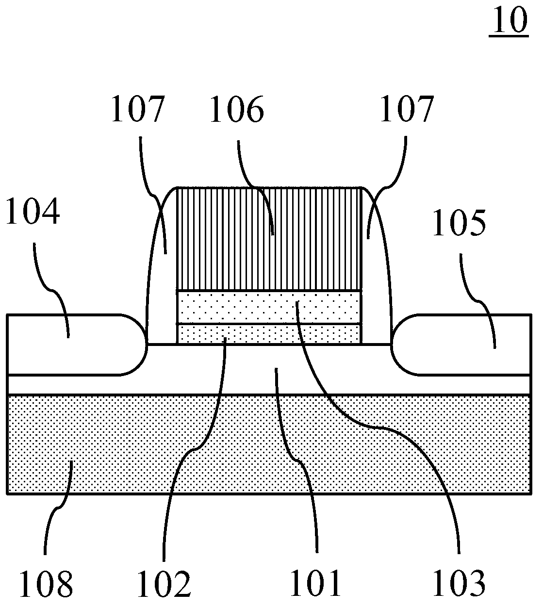
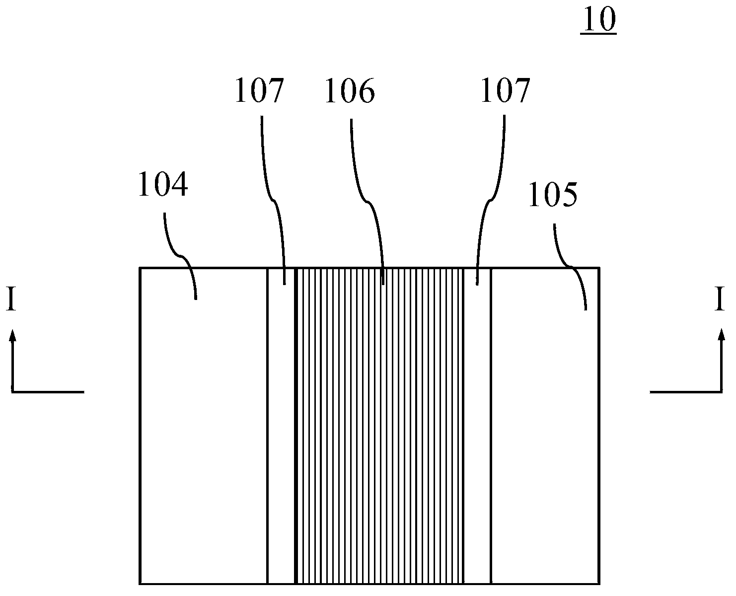
[0027] figure 1 It is the interface mode diagram of MOSFET (10). figure 2 is a top view model diagram of MOSFET (10). figure 2 The cross-sectional view of the I-I line in the middle, and figure 1 corresponding to the sectional view. Its structure is as follows:
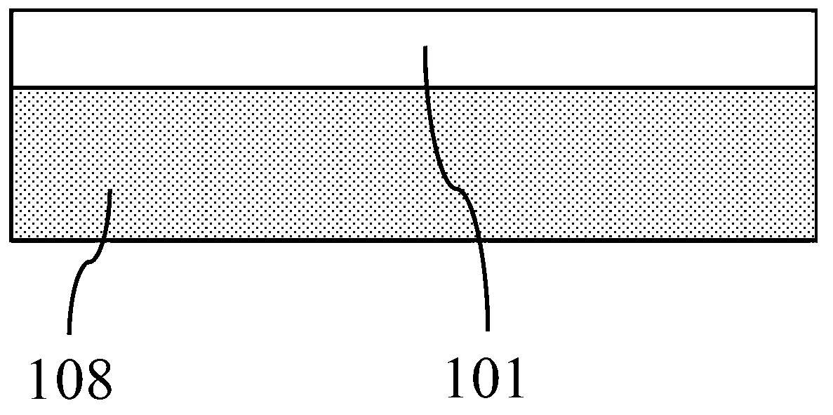
[0028] A substrate 108 with a Ge channel 101 thereon; an InAlP capping layer 102 positioned on the Ge channel 101; an insulating dielectric film 103 positioned on the InAlP capping layer 102; 106 a gate electrode, Located on the insulating dielectric film 103; a source 104 and a drain 105 are respectively located on both sides of the gate electrode 106; a first insulating spacer 107 is located between the gate and the source, The gate and the source are separated; the second insulating spacer 107, located between the gate and the drain, separates the gate and the drain.
[0029] Manufacturing process...
no. 2 example
[0037] The second example shows the fabrication of a p-type Ge channel MOSFET 20 with an InAlP capping layer.
[0038] Figure 9 It is the interface mode diagram of MOSFET20. Figure 10 is a top view model diagram of MOSFET (20). Figure 10 The cross-sectional view of the I'-I' line in the middle, and Figure 9 corresponding to the sectional view. Its structure is as follows:
[0039] a substrate 208 with a layer of relaxed Si 1-x Ge x (01-x Ge x(0<x<1) on the material. An InAlP capping layer 202, located on the Ge channel 201; an insulating dielectric film 203, located on the InAlP capping layer 202; 206, a gate electrode, located on the insulating dielectric film 203; a source An electrode 204 and a drain 205 are respectively located on both sides of the gate electrode 206; an insulating spacer 207 is located between the gate and the source, separating the gate and the source; another insulating spacer 207 , located between the gate and drain, separating the gate an...
PUM
| Property | Measurement | Unit |
|---|---|---|
| Thickness | aaaaa | aaaaa |
Abstract
Description
Claims
Application Information
 - R&D
- Intellectual Property
- Life Sciences
- Materials
- Tech Scout
- Unparalleled Data Quality
- Higher Quality Content
- 60% Fewer Hallucinations
Browse by: Latest US Patents, China's latest patents, Technical Efficacy Thesaurus, Application Domain, Technology Topic, Popular Technical Reports.
© 2025 PatSnap. All rights reserved.Legal|Privacy policy|Modern Slavery Act Transparency Statement|Sitemap|About US| Contact US: help@patsnap.com